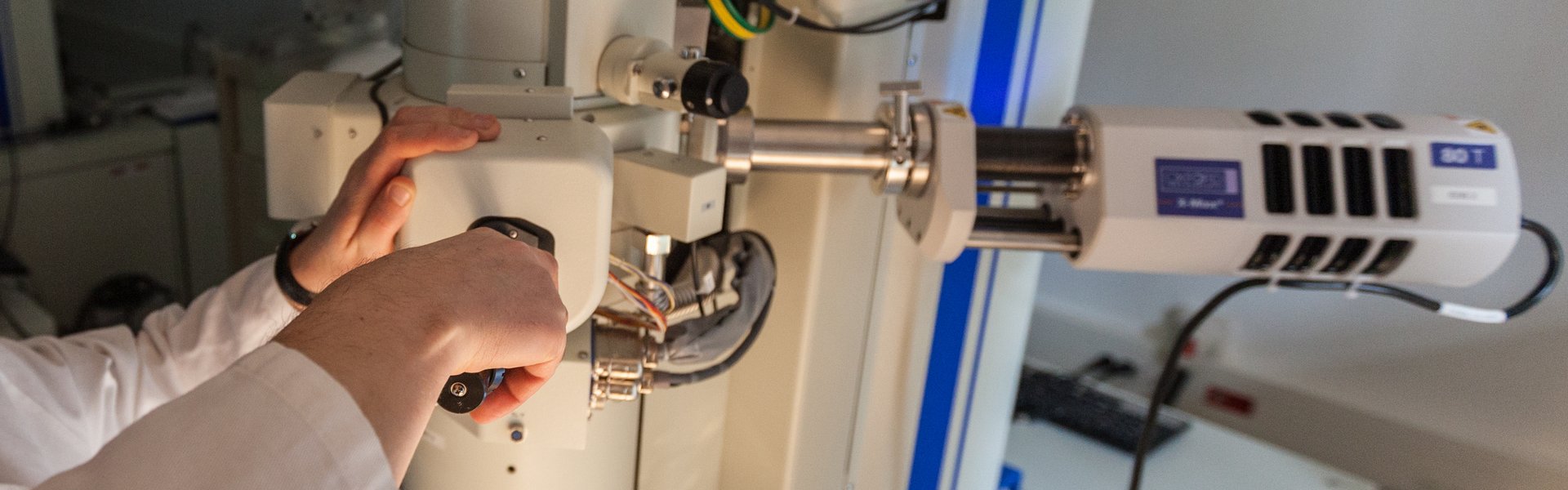
Research Highlights
Pennsylvania State University
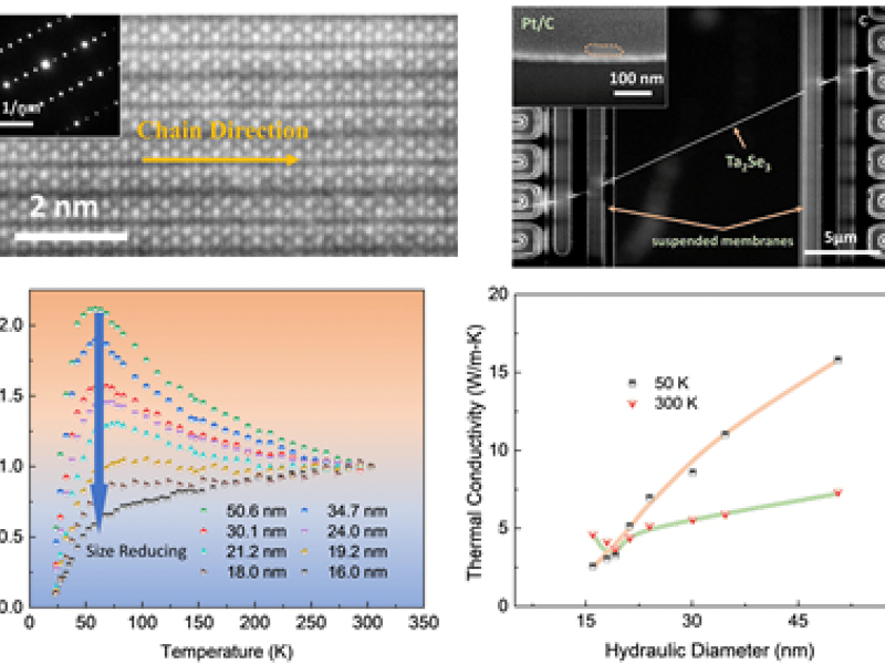
Elastic stiffening induces one-dimensional phonons in thin DMR-2039351 TaSe; nanowires
Z. Pan, Deyu Li, K. Wang, S. H. Lee, Z. Q. Mao
While previously, experimental studies of one-dimensional transform have been largely limited to earlier studies of thermal transport through single-walled carbon or boron nitride nanotubes, recent attempts have been made to probe thermal transport in quasi-1D van der Waals crystal nanowires, revealing interesting observations in the process.
Cornell University
Cleaning up a Quantum Material: from Quantum Enigma to Quantum Oscillations
B.J. Ramshaw, D.G. Schlom, K.M. Shen, L.F. Kourkoutis
Sr2RuO4 is the most disorder-sensitive superconductor known. It has also been a leading candidate for a novel type of quantum computer that would enable calculations to occur over much longer time scales before suffering decoherence than is the case for today’s superconductor-based quantum computers.
Cornell University
When Seemingly Passive Substrates are Active
X. Zheng, E. Gerber, J. Park, D. Werder, O. Kigner, E.-A. Kim, S. Xie, D.G. Schlom
Substrates traditionally play a supporting role for the thin films grown upon them by providing purely structural support. Nonetheless for monolayer-thick transition metal dichalcogenides , the substrate plays an active role by providing or removing charge from the TMD layer in which it is in intimate contact.
University of California, Santa Barbara
Fellows Cohort Selected
Javier Read de Alaniz , Heather Maynard
This cohort of more than 20 fellows marks the official start of the BioPACIFIC MIP in-house research and training programs.
Pennsylvania State University
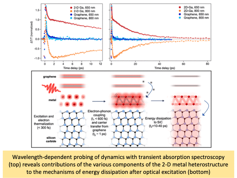
Atomic-Level Structure Determines Electron–Phonon Scattering Rates in 2-D Polar Metal Heterostructures
In this study, we measured the nonequilibrium carrier dynamics in an air-stable 2-D polar metal heterostructures. Using transient absorption spectroscopy, the mechanism for energy dissipation was determined to involve contributions from the various components of the heterostructure, including the 2-D metal layer, SiC substrate, and graphene capping layer.
Pennsylvania State University
Atomically thin half van der Waals materials via confinement heteroepitaxy
The process of stabilizing 2D superconductors via CHet can be applied to elements beyond p-block metals, opening opportunities to study unconventional properties that enable exploration of new physics and devices.
Pennsylvania State University
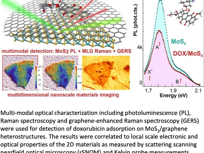
Multidimensional imaging reveals mechanisms controlling multimodal label-free biosensing in vertical 2DM heterostructures
T. Ignatova, S. Pourianejad , K. Schmidt, F. Aryeetey, S. Aravamudhan, S. Rotkin, B. Huet, J.M. Redwing
A multi-dimensional optical imaging technique that combines scattering was developed to map subdiffractional distributions of doping and strain in MoS2 and MoS2 /graphene vertical heterostructures. The variations in doping and strain were correlated to electronic properties and were used to understand the behavior of biosensors fabricated using the 2D material.
Pennsylvania State University
Topological Hall Effect in Topological Insulator/Magnetic Insulator Bilayer
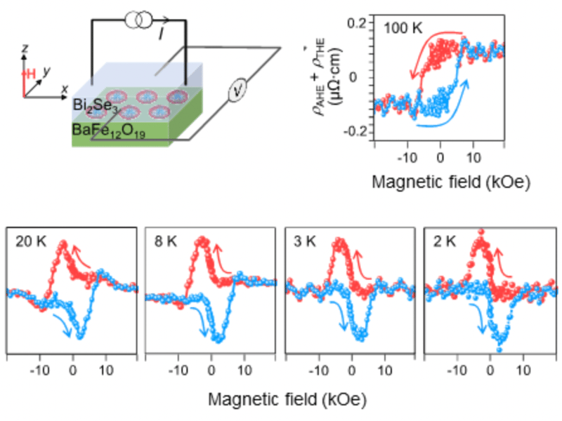
The topological Hall effect (THE) is a phenomenon that is a consequence of a Berry phase created by spin textures in real space. Interfacing a topological insulator with a magnetic insulator provides a model platform for studying this phenomenon in a well-controlled manner. This paper reports the first clear evidence for the THE in heterostructures that combine a model topological insulator (Bi2Se3) with a ferromagnetic insulator (BaFe12O19).
Pennsylvania State University
Evidence of nested quasi-one-dimensional Fermi surface and decoupled charge-lattice orders in layered TaTe2
Y. Lin, M. Huber, K. M. Siddiqui, L. Moreschini, P. Ai, S. Rajpurohit, L. Tan, j.D. Denlinger, A Lanzara, D. H. Eilbott, L Moreschini, Y.L. Zhu, Z.Q. Mao
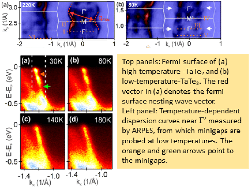
Prof. Lanzara' group at Lawrence Berkeley National Laboratory recently studied the anomalous CDW phase transition of TaTe using APES and low-energy electron diffraction. Their data reveal the presence of a surprising quasi- one-dimensional Fermi surface with nesting condition. They find that the wave vectors of the Fermi surface nesting and periodic lattice distortion are different, suggesting the decoupled formation between charge and lattice orders. This work provides routes for forging unconventional CW phases and charge- lattice entanglement that would otherwise not be available in materials with fixed dimensionality.
Pennsylvania State University
Remote Epitaxy of 3D functional semiconductors and oxides using Graphene as the Interface layer
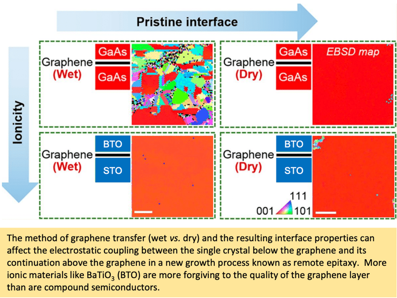
In this highlight, 2DCC and PARADIM team up to work with the inventor of remote epitaxy, Prof. Kim (MIT), to unveil the respective roles and impacts of the substrate material, graphene, substrate–graphene interface, and epitaxial material for electrostatic coupling of these materials, which governs cohesive ordering and can lead to single crystal epitaxy in the overlying film.
Showing 161 to 170 of 237