Research Highlights
Pennsylvania State University
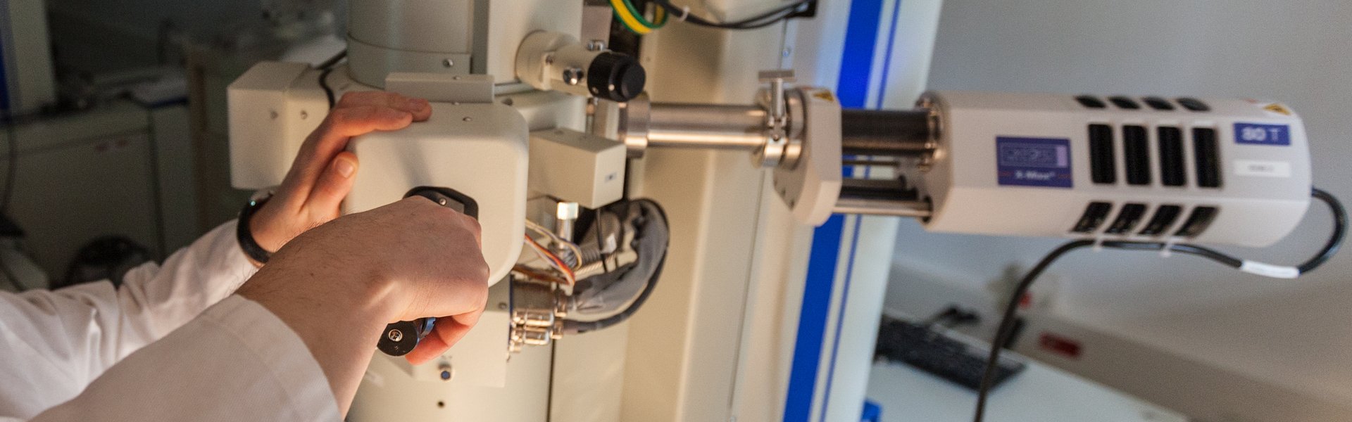
Growth of ultrathin Pt layers and selenization into PtSe2 by molecular beam epitaxy
Among the high-mobility two-dimensional transition metal dichalcogenides PtSe2 is of particular interest due to its record high carrier mobility of 1,000 cm2/Vs, sizeable band gap and air stability to address the current need for low-power, high-performance and ultra-thin body electronics.
Pennsylvania State University
Benchmarking monolayer MoS2 and WS2 field-effect transistors
To assess the potential of transition metal dichalcogenides (TMDs) for future circuits, it is important to study the variation in key device parameters across a large number of devices. Here we benchmark device-to-device variation in field-effect transistors (FETs) based on wafer-scale monolayer MoS2 and WS2.
University of California, Santa Barbara
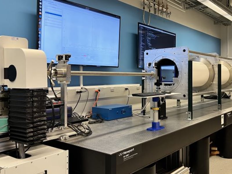
BioPACIFIC MIP Advanced X-ray Available to Users
New X-ray Facility Brings Synchrotron-level Capabilities to BioPACIFIC MIP
Pennsylvania State University
Closing the Loop on the 2D Materials Genome
The Two-Dimensional Crystal Consortium closely couples experimental synthesis and measurement with theoretical and computational work to close the discovery loop on the growth and characterization of 2D materials.
Pennsylvania State University
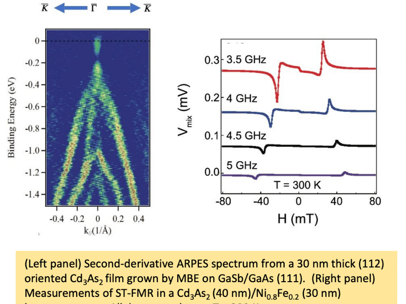
Spin-charge interconversion in a Dirac semimetal
This research explores room-temperature measurements of SCI at the interface between an archetypal Dirac semimetal (Cd3As2) and a conventional metallic ferromagnet (Ni0.8Fe0.2).
Pennsylvania State University
A roadmap for electronic grade 2D materials
2-dimensional materials hold promise for next-generation electronics. However, in order to realize 2D-based technologies, key milestones must be identified and met. This article identifies areas of research which are fundamentally required for achieving electronic grade 2D materials and brings together experts in these respective areas to discuss key challenges.
Pennsylvania State University
Quantification of defects engineered in single layer MoS2
Atomic defects are controllably introduced in suspended single layer molybdenum disulfide (1L MoS2) using helium ion beam. Vacancies exhibit one missing atom of molybdenum and a few atoms of sulfur. Quantification was done using a Scanning Transmission Electron Microscope (STEM) with an annular detector. Experimentally accessible inter-defect distance was employed to measure the degree of crystallinity in 1L MoS2. Correlation between the appearance of an acoustic phonon mode in the Raman spectra and the inter-defect distance was established, which introduces a new methodology for quantifying defects in 2D materials.
Showing 231 to 237 of 237