
Latest News
Highlight ·
Pennsylvania State University
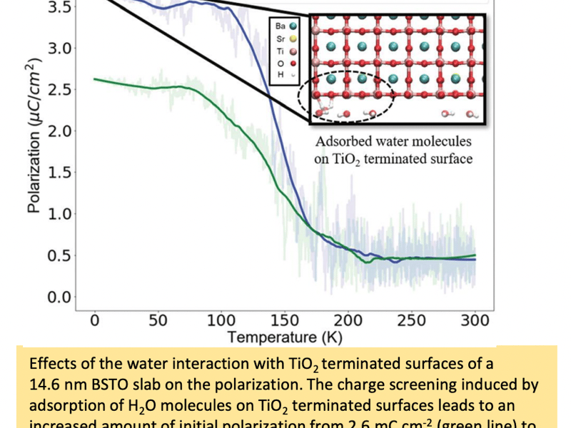
Understanding the physical chemistry properties of BaxSr1-xTiO3 using ReaxFF based Molecular Dynamics Simulations
In order to expand the ReaxFF capability for support material simulations, the 2DCC group has extended a previously developed ReaxFF parameter set for BaTiO3 to SrTiO3 (STO) – a highly relevant support material for 2D-chalcogenide growth.
Highlight ·
Cornell University
“Band-Structure Engineering” of Quantum Materials to Create a new Superconductor
J.P. Ruf, H. Paik, N.J. Schreiber, H. P. Nair, L. Miao, J.K. Kawasaki, J.N. Nelson, B.D. Faeth, Y. Lee, B.H. Goodge, B. Pamuk, C.J. Fennie, L.F. Kourkoutis, D.G. Schlom, K.M. Shen
One Materials-by-design commonly starts with first principles theory to identify materials with desired properties. The significant energetic contribution of electron-electron interactions, however, makes it difficult for theory to accurately predict quantum materials. Experimental tools like ARPES that measure electronic band structure directly used in combination with synthesis tools like MBE make it possible to enter the materials-by-design loop from a different on-ramp and navigate quantum materials to achieve desired properties.
Highlight ·
Pennsylvania State University
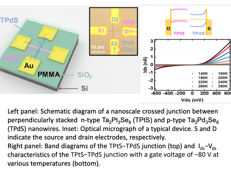
Tunneling Effects in Crossed Ta2Pt3Se8−Ta2Pd3Se8 Nanowire Junctions: Implications for Anisotropic Photodetectors
This study not only offers a way to build nanoscale junctions but also provides fundamental understandings of the electronic and optoelectronic properties of vdW nanowires and their heterojunctions.
Highlight ·
Pennsylvania State University
New Theory Tools for Modeling Growth of TMD Materials
The first ReaxFF force field developed for 2D-WSe2 provides the community with a highly efficient means that describe material growth, phase transitions, defect formation and migration and thus can provide valuable atomistic insights into experimental efforts on growth, phase, and defect engineering as a function of the local chemical environment. This potential can elucidate further the morphological evolution of monolayers in different environments in terms of loading conditions and defect concentrations/distributions. Interactions between vacancies and ripples in a 2D layers (“ripplocations”) suggest that vacancies could stabilize buckled structures by modulating the strain energy and possibly open a venue for sweeping out undesirable defects such as vacancies from 2D WSe2.
Highlight ·
Pennsylvania State University
Coupling Distinct Defect Species In 2D Crystals
Doping modulates the electronic, chemical, and mechanical properties of materials. For a two-dimensional tungsten disulfide, although an isolated molybdenum substitution only perturbs the host lattice negligibly, it couples strongly to common lattice defects such as sulfur vacancies, as verified by state-of-the-art electron microscopy and atomistic modeling techniques.
Highlight ·
Pennsylvania State University
Origami Without Fingers
Origami with regular paper can produce a limitless number of fascinating, beautiful and useful shapes, but we lack “fingers” at the nanoscale to guide the folding. Researchers in the Two-Dimensional Crystal Consortium at Penn State have conceived and simulated a novel way to “program” a folding pattern by patterning the nanoscale sheet with complementary regions of n-type and p-type doping.
Highlight ·
Pennsylvania State University
Growth of ultrathin Pt layers and selenization into PtSe2 by molecular beam epitaxy
Among the high-mobility two-dimensional transition metal dichalcogenides PtSe2 is of particular interest due to its record high carrier mobility of 1,000 cm2/Vs, sizeable band gap and air stability to address the current need for low-power, high-performance and ultra-thin body electronics.
Highlight ·
Pennsylvania State University
Benchmarking monolayer MoS2 and WS2 field-effect transistors
To assess the potential of transition metal dichalcogenides (TMDs) for future circuits, it is important to study the variation in key device parameters across a large number of devices. Here we benchmark device-to-device variation in field-effect transistors (FETs) based on wafer-scale monolayer MoS2 and WS2.
Highlight ·
University of California, Santa Barbara
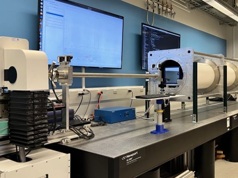
BioPACIFIC MIP Advanced X-ray Available to Users
New X-ray Facility Brings Synchrotron-level Capabilities to BioPACIFIC MIP
Highlight ·
Pennsylvania State University
Closing the Loop on the 2D Materials Genome
The Two-Dimensional Crystal Consortium closely couples experimental synthesis and measurement with theoretical and computational work to close the discovery loop on the growth and characterization of 2D materials.
Showing 351 to 360 of 363