Latest News

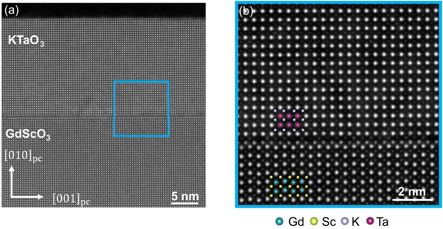
Figure 1: Atom resolution scanning transmission electron microscopy (STEM) image of a KTaO3 thin film on GdSc O3 and zoomed view on the interface with the substrate. Figure 2: X-ray diffraction ) X-ray diffraction θ-2θ scan of a high-quality KTaO3 thin film showing 00l peaks and Laue fringes.
Highlight · Feb 2, 2023
Cornell University

The Multiplicative Effect of Knowledge Sharing

Kaveh Ahadi (NCSU), M.D. Williams (Clark Atlanta University), and D.A. Muller and D.G. Schlom (Cornell University).
This publication marks the first time that KTaO3 films have been grown by MBE. The approach used overcame the technical challenges of (1) the low vapor pressure of tantalum (normally impossible in a stable MBE effusion cell due to the low vapor pressure of tantalum) and (2) the safety issues of safely handling potassium, which is highly flammable. The resulting films have the highest structural quality of any KTaO3 films ever grown judging from the narrowness of the x-ray diffraction rocking curves and rather featureless microstructure revealed by STEM.
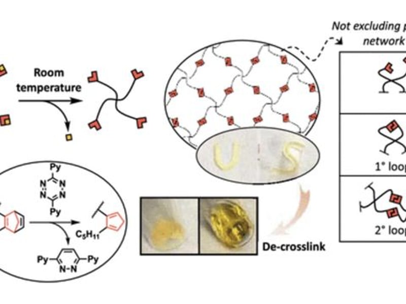
Sufficient isolation of a well-defined 4-arm cyclopentadiene derivative via tetrazine cascade reactions leads to controlled synthesis of a shape-memory and degradable single-component Diels–Alder homopolymer network.
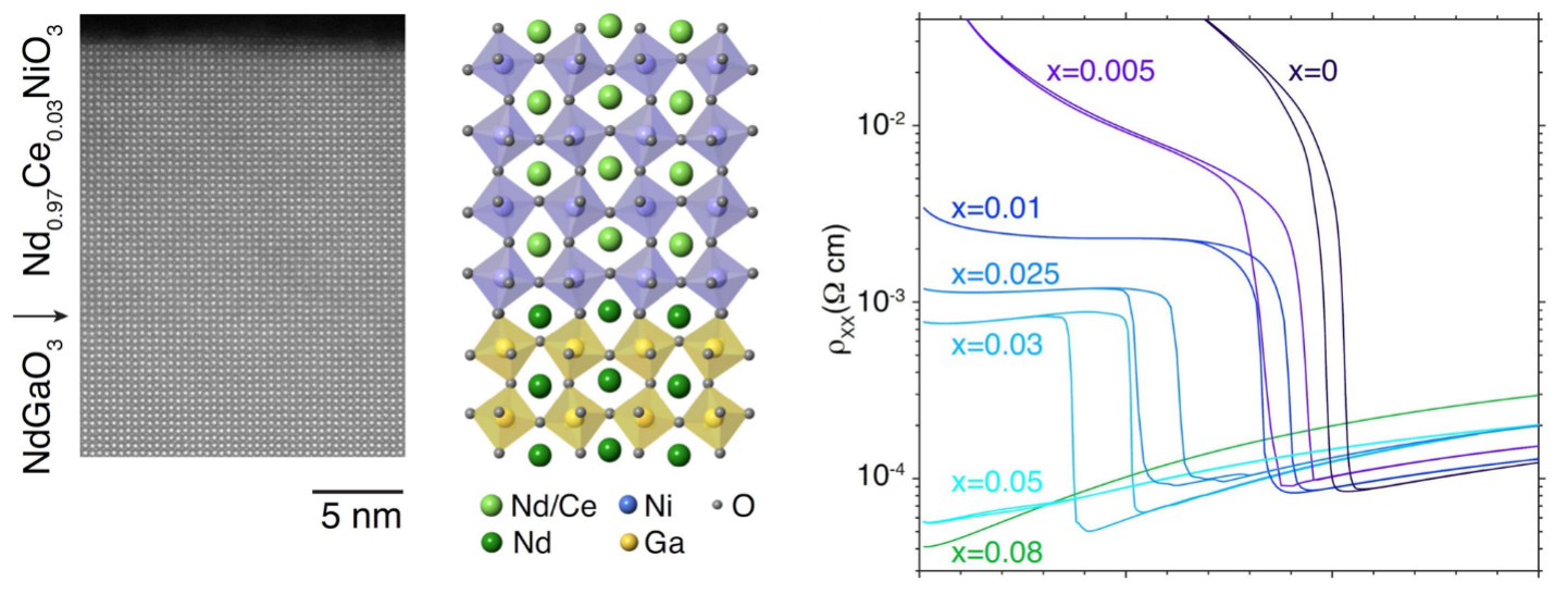
Figure 1: (Left) Atom resolution STEM image of the new material and its interface with the substrate, Structure model shown for comparison. (Right) Resistivity vs. temperature for CexNd1-xNiO3 films synthesized on NdGaO3. Cerium substitution results in qualitative changes in the transport properties of the films. The parent compound NdNiO3 shows a metal-insulator transition at ~200 K with a resistivity increase of about five orders of magnitude. For intermediate cerium doping the resistivity increases but recovers metallic behavior, indicative of a metal-metal transition. Figure 2: Electronic and magnetic phase diagram extracted in this study on films synthesized on NdGaO3 substrates. AFM and PM refer to antiferromagnetic and paramagnetic, respectively. The symbols indicate electronic transport (◊), RXS (○) and ARPES (□).
Highlight · Jan 30, 2023
Cornell University

PARADIM – an Incubator for Collaborations III

Julia A. Mundy, I. El Baggari (Harvard University), Antia S. Botana (Arizona State University), John T. Heron (University of Michigan), A. Lanzara & Luca Moreschini (Advanced Light Source)
A team of experimentalists and theorists connecting at PARADIM have discovered a new antiferromagnetic metal. Their discovery adds to the rich variety of physical properties exhibited by rare-earth nickelates: superconductivity (previously discovered by the core members of this team), metal-insulator transitions, and antiferromagnetic insulators. This latest discovery provides additional insights into the coupling of spin, charge, and lattice degrees of freedom when these elements are combined.
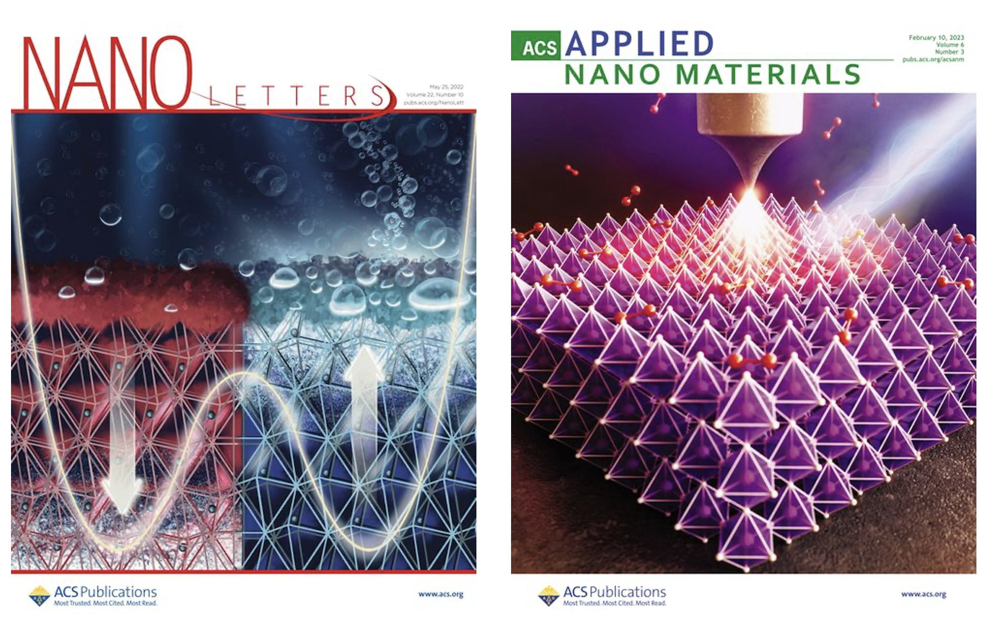
Figure 1: Journal covers highlighting the recent work by Pedram Abbasi, David P. Fenning, and collaborators on epitaxially thin films of barium titanate (BaTiO3)—a ferroelectric model compound—and the impact of polarization on the hydrogen evolution reaction [1, 2].
Highlight · Jan 18, 2023
Cornell University

Modulating Catalytic Activity using a Ferroelectric

T.A. Pascal and D.P. Fenning (University of California—San Diego), D.G. Schlom (Cornell University), and V. Rose (Argonne National Laboratory)
An emerging opportunity for ferroelectrics is to modulate catalytic activity. Such behavior has been reported in a prior PARADIM publication by this same user utilizing MBE-grown epitaxial BaTiO3 thin films with atomically sharp interfaces as model surfaces to demonstrate the effect of ferroelectric polarization on the electronic structure, intermediate binding energy, and electrochemical activity toward the hydrogen evolution reaction (HER).
BioPACIFIC MIP’s project scientist Dr. Morgan Bates and Dr. Panchanathan, discuss how automation can help accelerate research
Highlight · Jan 1, 2023
University of California, Santa Barbara

National Science Foundation director visits BioPACIFIC MIP facilities
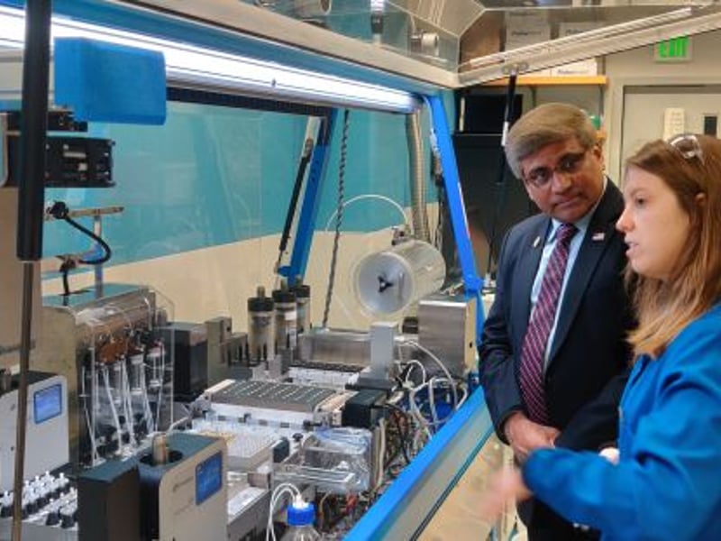
In a recent visit to the University of California, Santa Barbara (UCSB), Dr. Sethuraman Panchanathan, Director of the National Science Foundation (NSF), explored the cutting-edge facilities available on campus.
Towards a mechanistic understanding of the formation of 2D-GaNx via MOCVD
Highlight · Dec 29, 2022
Pennsylvania State University

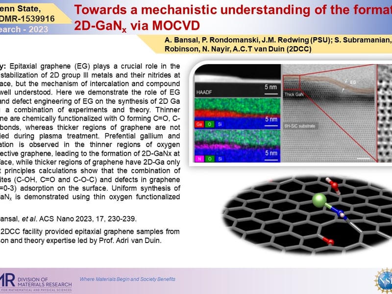
Towards a mechanistic understanding of the formation of 2D-GaNx via MOCVD

A. Bansal, P. Rondomanski, J.M. Redwing (PSU); S. Subramanian, S. Kumari, J.A. Robinson, N. Nayir, A.C.T van Duin (2DCC)
Epitaxial graphene (EG) plays a crucial role in the confinement and stabilization of 2D group III metals and their nitrides at the EG/SiC interface, but the mechanism of intercalation and compound formation is not well understood.
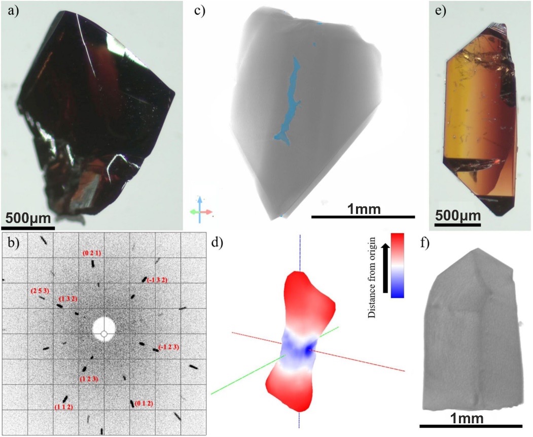
Figure 1: Voids in rutile germanium oxide, r-GeO2. a) A single crystal of rutile GeO2 grown using a flux with a cooling rate of 3 °C/h. b) Laue diffraction image of the crystal along the [011] direction. c) A representation of a crystal from the same batch as (a) generated from μCT data with voids present (highlighted blue). d) A 3D rose diagram of the star volume distribution of the voids. The data was aligned such that the void shows a preferential orientation parallel to the [011] direction of the crystal axis. The image is colored according to the distance from the origin. e) A different crystal of rutile GeO2 grown using a flux with a cooling rate of 0.5 °C/h. f) A rendering of a crystal from the same batch as in (e) showing no detectable voids.
Highlight · Dec 29, 2022
Cornell University

X-ray micro-computed tomography informs materials discovery

John T. Heron (U. of Michigan) and Tyrel M. McQueen (JHU)
Here, members of PARADIM’s in-house research team collaborated with external users and summer school participants on case studies of µCT informing materials design of electronic and quantum materials, benefitting the characterization of inclusions, twinning, and low-angle grain boundaries and optimizing crystal growth processes. The work discusses recent improvements in µCT instrumentation that enable elemental analysis and orientation to be obtained on crystalline samples.
Electrical Control of Inversion Symmetry
Highlight · Dec 19, 2022
Cornell University

Electrical Control of Inversion Symmetry

R. Ramesh (UC Berkeley), M. Fiebig, N.A. Spaldin (ETH Zurich), D.A. Muller, D.G. Schlom (Cornell University)

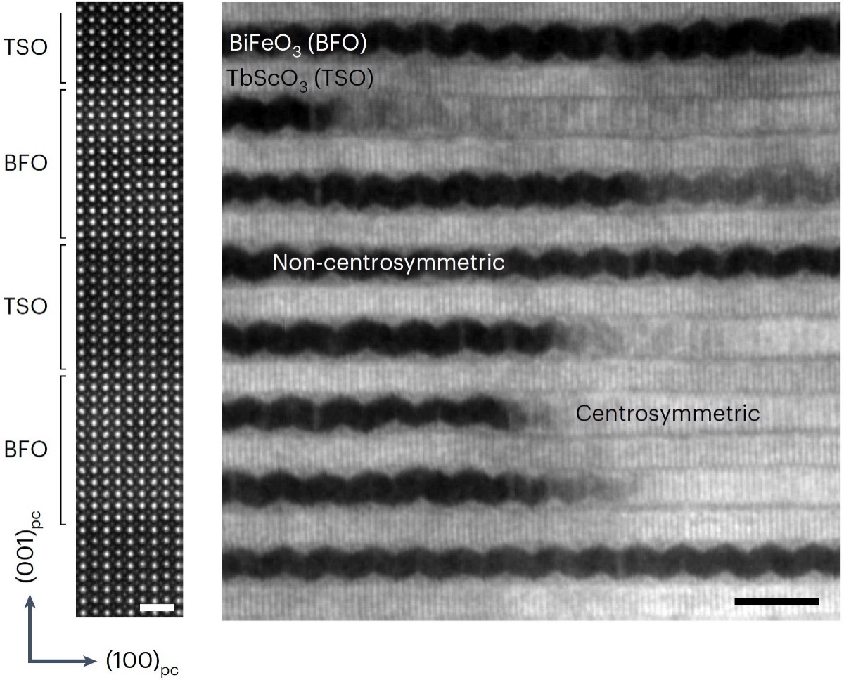
Symmetry in crystalline materials largely dictates their properties and new functionalities can arise when inversion symmetry is broken and disappear when it is restored. PARADIM users have made a new material in which by applying a voltage they can "turn off" and "turn on" the inversion symmetry of the atomic arrangement. Inversion symmetry is what happens when you turn an object inside out.
Courtesy of 2DCC News
News · Dec 9, 2022
Pennsylvania State University

2D material may enable ultra-sharp cellphone photos in low light
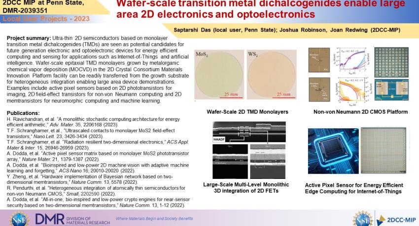
Researchers at Penn State developed a novel active pixel sensor using molybdenum disulfide, enabling sharper, energy-efficient cellphone photography and IoT sensors. This technology reduces energy costs and enhances image processing, allowing for clearer photos in low-light and adverse conditions, contributing to sustainability in photography and smart manufacturing.
Wafer-scale transition metal dichalcogenides enable large area 2D electronics and optoelectronics
Highlight · Dec 8, 2022
Pennsylvania State University

Wafer-scale transition metal dichalcogenides enable large area 2D electronics and optoelectronics

Saptarshi Das (local user, Penn State); Joshua Robinson, Joan Redwing (2DCC-MIP)

Ultra-thin 2D semiconductors based on monolayer transition metal dichalcogenides (TMDs) are seen as potential candidates for future generation electronic and optoelectronic devices for energy efficient computing and sensing for applications such as Internet-of-Things and artificial intelligence.