Research Highlights
Jul 26, 2021
University of California, Santa Barbara
New Photopatterning Platform
Javier Read de Alaniz
Adducts of cyclopentadienone–norbornadiene (CPD–NBD) have been developed and utilized in Diels–Alder based photopatterning of soft materials.
Jul 6, 2021
Pennsylvania State University
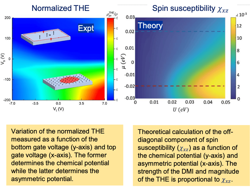
Mapping the phase diagram of the quantum anomalous Hall and topological Hall effects
The interplay between topology in momentum space and topology in real space creates a vibrant playground for studying emergent phenomena in condensed matter physics.
Jun 30, 2021
Cornell University
Quantification of Interfacial Electron-Phonon Coupling from Photoemission Replica Bands in a High-Tc Superconductor
The observation of replica bands by angle-resolved photoemission spectroscopy enables the study of electron-phonon coupling at low carrier densities, particularly in monolayer FeSe/SrTiO3. Theoretical work suggests that the electrons in the ultra-thin FeSe layer couple to optical phonons in the SrTiO3 substrate that thereby contributes to the enhanced superconducting pairing temperature. So far, the inherent fragility of such single-layer thick materials and the weak intensity of replica features has limited the quantitative evaluation of their nature.
Jun 25, 2021
Cornell University
PARADIM – an Incubator for Collaborations
Important applications like ultrashort pulsed lasers, sensors, laser amplifiers, and digital optical information processing, depend on materials with nonlinear optical properties—that is the material’s nonlinear interaction with electromagnetic waves, :e.g.:, light.
Jun 18, 2021
Cornell University
Cryo-STEM Unveils Electronic Order at the Atomic Scale
Lena F. Kourkoutis, Elisabeth A. Nowadnick, Harold Y. Hwang
In quantum materials, electrons can interact strongly with each other and with the atomic lattice, giving rise to novel electronic states with functionalities not achievable in conventional materials. At the atomic scale, the local crystal symmetries are governed by variations in the charge distribution and subtle atomic displacements, dramatically affecting the material’s properties.
Jun 10, 2021
Cornell University
Discovery of “Pseudogap” Behavior in a Monolayer Thick High-Temperature Superconductor
Darrell G. Schlom, Kyle M. Shen
Members of PARADIM’s in-house research team have employed a combination of angle-resolved photoemission spectroscopy and in situ resistivity measurements to simultaneously probe both the electronic states and superconducting behavior of pristine monolayer FeSe/SrTiO3.
Jun 10, 2021
Cornell University
Discovery of “Pseudogap” Behavior in a Monolayer Thick High-Temperature Superconductor
The ability to produce pristine atomic interfaces by growing the structures atom-by-atom :via: molecular beam epitaxy has opened the door to an entirely new class of emergent phenomena in the form of interface quantum materials. One remarkable example of such a material system is the interface between monolayer iron selenide (FeSe) films and SrTiO:3:, where superconductivity can be observed at dramatically higher temperatures compared to 8 K of bulk FeSe. So far, the inherent fragility of such ultra-thin layers has prevented the direct study of superconductivity :via: direct probes like electrical resistivity.
Jun 3, 2021
Cornell University
Remote Epitaxy of 3D functional semiconductors and oxides using Graphene as the Interface layer
H. Paik:, :S. Xie:, H. Shin, C. Choi, J.H. Le, :C. Dong:, :J.A. Robinson (2DCC):, :J.-H. Lee:, J.-H. Ahn, G.Y. Yeom, :D.G. Schlom (PARADIM):, J. Kim (MIT):Project Summary::Remote epitaxy has drawn attention as it offers epitaxy of functional materials that can be released from the substrates with atomic precision, thus enabling production and heterointegration of flexible, transferrable, and stackable freestanding single-crystalline membranes. In this highlight, 2DCC and PARADIM team up to work with the inventor of remote epitaxy, Prof. Kim (MIT), to unveil the respective roles and impacts of the substrate material, graphene, substrate–graphene interface, and epitaxial material for electrostatic coupling of these materials, which governs cohesive ordering and can lead to single-crystal epitaxy in the overlying film.
May 31, 2021
University of California, Santa Barbara
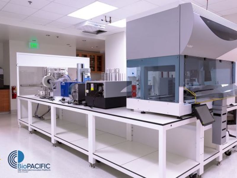
Living Biofoundry Becomes Available
The BioPACIFIC MIP Living Biofoundry (LBF) has been installed at UCLA and is now available to users.
May 21, 2021
Cornell University
The Highest Resolution Microscope, enabled by a new detector technology, reaches an ultimate resolution limit – the vibrations of atoms themselves
Electron microscopy is a widespread and often essential tool for structural and chemical analysis at the atomic level. Image resolution is dominated by the energy (or wavelength) of the electron beam and the quality of the lens. By combining our new design of electron microscope pixel array detector (EMPAD), which has the dynamic range to record the complete distribution of transmitted electrons at every beam position and a phase retrieval algorithm to process the data, PARADIM’s in-house research team has increased the spatial resolution well beyond the traditional lens limitations, setting a world record in 2018 for the highest resolution microscope (0.39 Å Abbe resolution [1]) at the same dose and imaging conditions where conventional imaging modes reach only 0.98 Å. The EMPAD is the culmination of over a decade of detector development at Cornell, supported by NSF (through CHESS, CCMR), DOE, the WM Keck Foundation, and the Kavli Institute, and has been commercially licensed by ThermoFisher Scientific and is now manufactured and sold at scale.
Showing 121 to 130 of 237