Latest News
Highlight · Nov 1, 2025
Cornell University
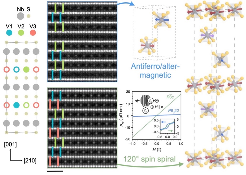
Unconventional Superlattice Ordering in Intercalated Transition Metal Dichalcogenide
UC Berkeley researchers show V1/3NbS2 can crystallize into two ordered intercalant superlattices (ABAB and ABC) with distinct magnetism and electronics. One is metallic with altermagnetism; the other semimetallic noncollinear antiferromagnet with potential topological properties. This enables tunable magnetic/electronic states for spintronics and topological devices.
Highlight · Sep 1, 2025
Cornell University
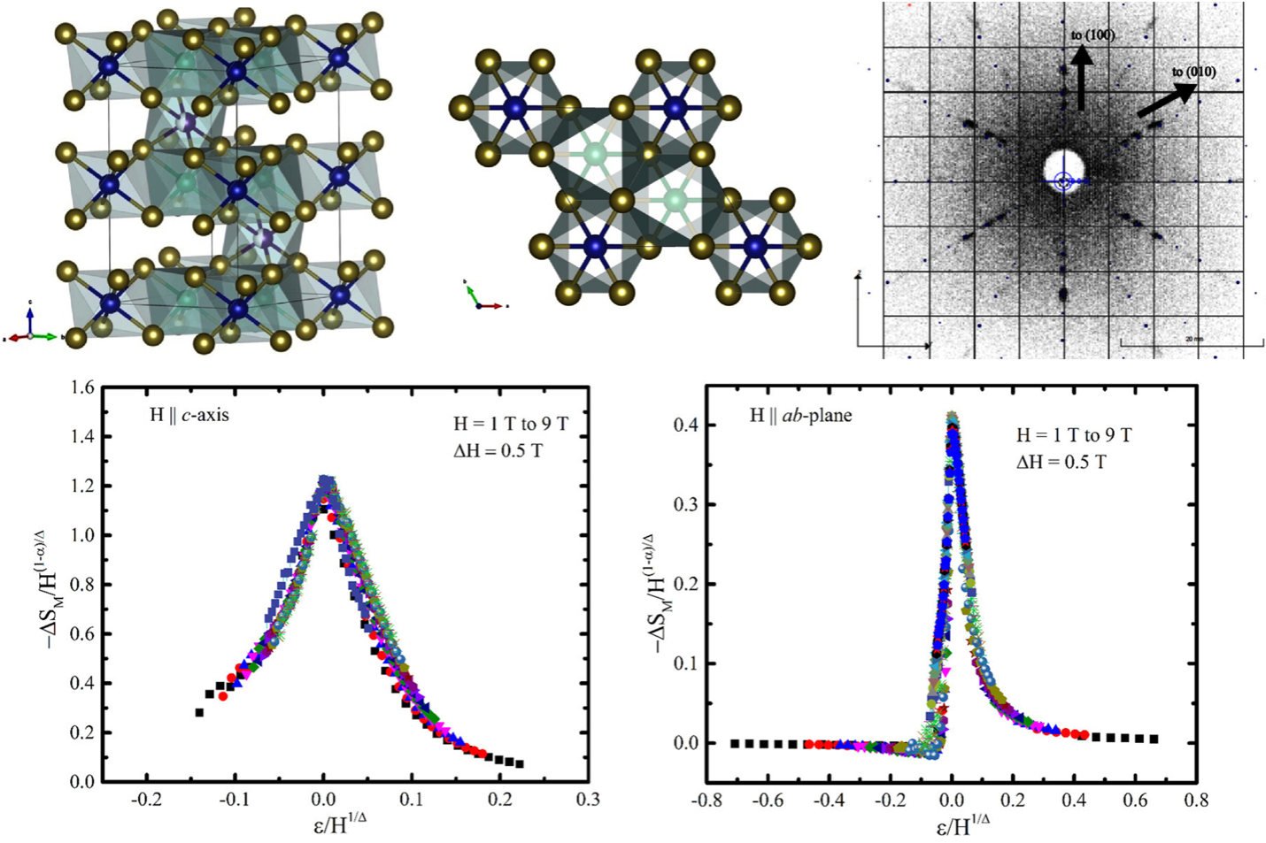
Intertwined Phases and Magnetocaloric Anisotropy in Cr2+xTe4
PARADIM researchers (Guchhait, Howard Univ.) explored Cr-Te layered phases CrTe2–Cr3Te4, synthesizing compositionally precise Cr2+xTe4 crystals to study magnetic properties. They found Cr2Te3 exhibits a large, anisotropic magnetocaloric effect at 170 K; thin films show ordering near 280 K, promising room-temperature magnetocaloric devices. CVT growth enabled precise interstitial ordering.

Highlight · Sep 1, 2025
Cornell University
“Infinite Layer” Nickelates Superconduct even without Doping?
PARADIM's In-House team reports superconductivity with onset up to 11 K in high-crystallinity, undoped NdNiO2 thin films. Superconductivity appears when residual resistivity drops below the NiO2 sheet quantum resistance, suggesting intrinsic, clean-limit behavior akin to cuprates. Apical oxygens could also contribute; film quality is key.
Highlight · Sep 1, 2025
Cornell University
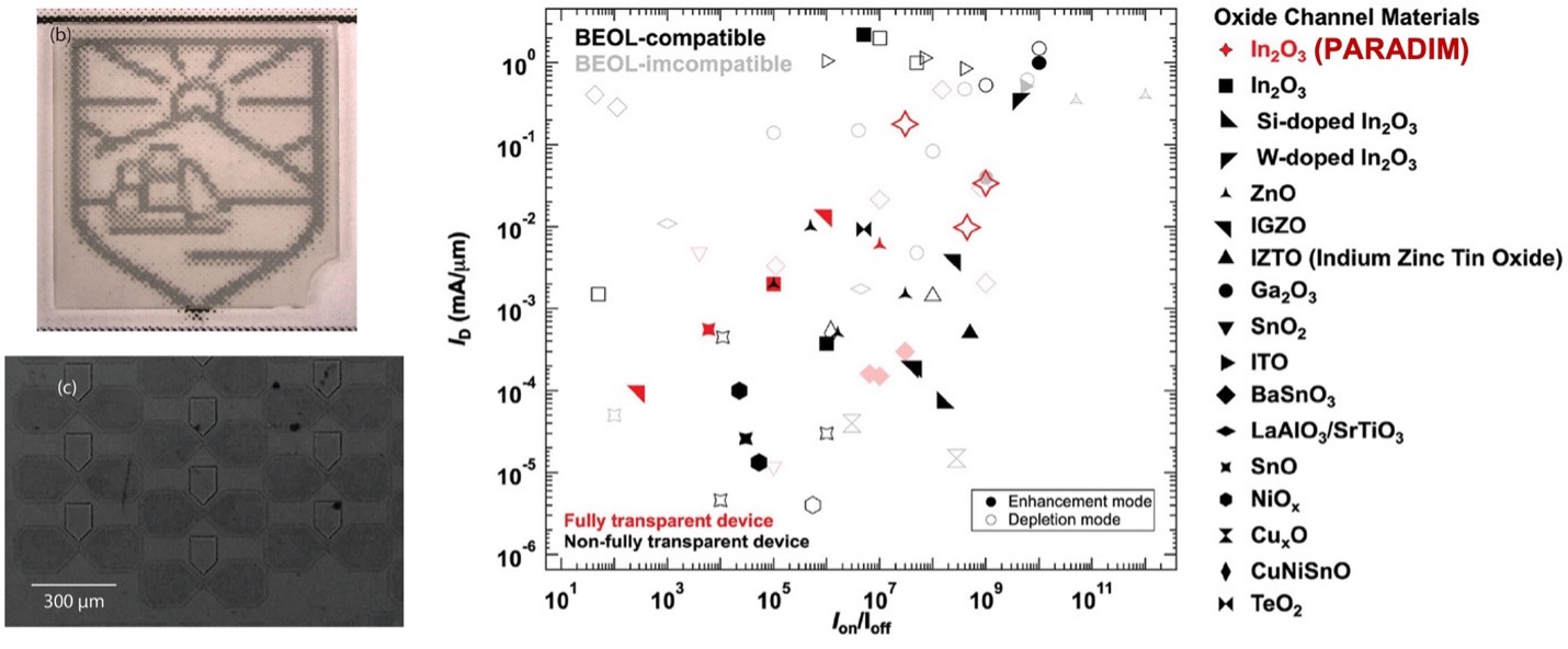
Fully transparent transistors fabricated at Back-End-of-Line conditions
PARADIM’s Highlight #109 reports that suboxide MBE (S-MBE) enables epitaxial In2O3 at BEOL temperatures, yielding the highest-performance fully transparent oxide TFTs to date. The pre-oxidized In2O beam provides exceptional crystal quality and BEOL-compatible devices, accelerating open collaboration and 22 publications across 34 PARADIM projects.
News · Aug 21, 2025
University of California, Santa Barbara
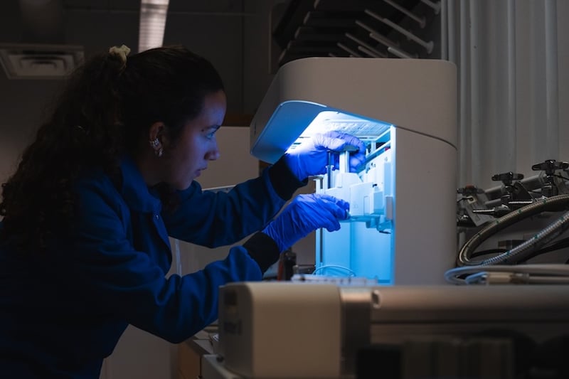
UC Santa Barbara, UCLA’s BioPACIFIC MIP earns renewed NSF support to accelerate AI-driven biobased materials innovation
The U.S. National Science Foundation has renewed funding for BioPACIFIC MIP — Biomaterials, Polymers and Advanced Constructs from Integrated Chemistry Materials Innovation Platform — a collaboration between UC Santa Barbara and UCLA that provides a unique scientific ecosystem for the United States. This $19.8 million renewal empowers BioPACIFIC MIP to continue advancing the frontier of biobased materials, uniting synthetic biology, chemistry, automation and artificial intelligence to reshape how materials are discovered, designed and deployed.
Highlight · Aug 1, 2025
Cornell University
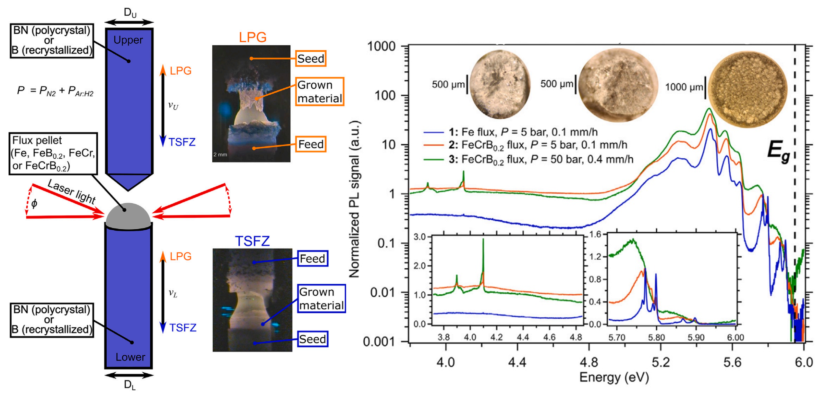
Growth of hexagonal BN crystals by traveling-solvent floating zone
PARADIM Highlight #108 reports scalable growth of high-purity hexagonal boron nitride (h-BN) crystals via solvent laser pedestal and traveling-solvent floating-zone methods, achieving 3–5 mm diameters and multi-mm lengths. This enables larger, defect-minimized h-BN for 2D devices; funded by PARADIM, with collaborators at KU, Texas Tech, Montpellier, UCSB, JHU.
News · Jul 29, 2025
University of California, Santa Barbara
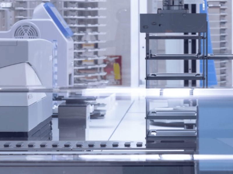
Collect plasmids — fast, easy and consistently — with BioPACIFIC MIP at UCLA Automated System
The BioPACIFIC MIP at UCLA offers an automated high-throughput system for isolating plasmid DNA from microbes. This platform enhances efficiency in research across biotechnology and life sciences, processing up to 96 minipreps simultaneously with minimal human intervention. Researchers can achieve high-purity plasmids swiftly, supporting various applications.
News · Jul 25, 2025
Pennsylvania State University
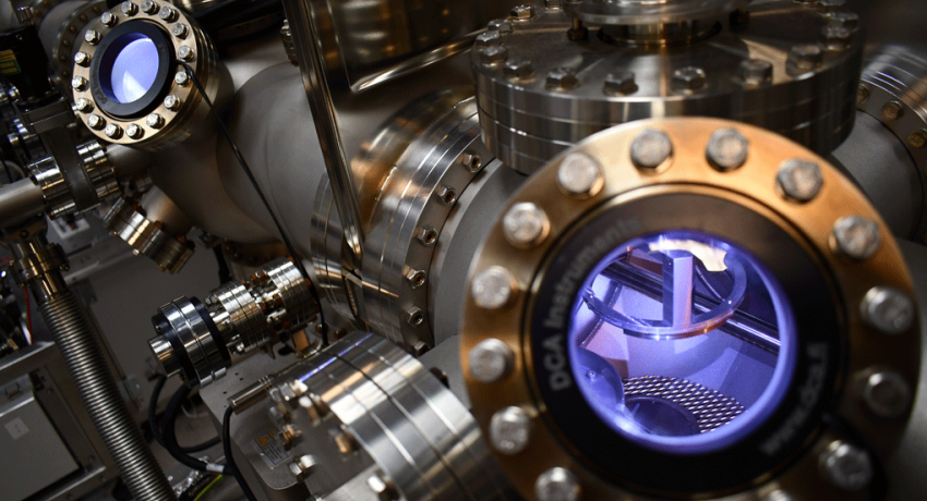
Tools of Discovery: How new equipment is powering research breakthroughs at Penn State
Penn State's advanced lab tools, including a unique double-crucible vertical Bridgman furnace and in situ testing capabilities, are enabling breakthroughs in materials science. These innovations allow researchers to grow ultra-pure crystals and study material behaviors in real-world conditions, paving the way for future technologies like advanced computing and flexible electronics.
News · Jun 13, 2025
Pennsylvania State University
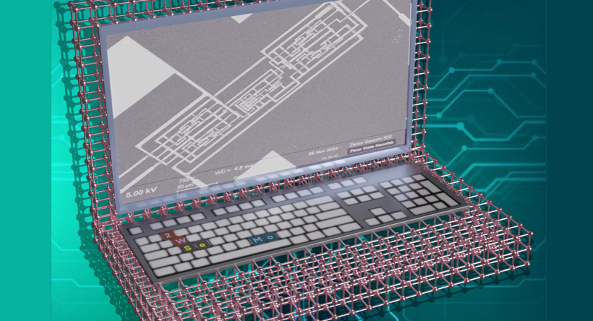
World’s first 2D, non-silicon computer developed
Researchers at Penn State have developed a CMOS computer using two-dimensional materials, marking a significant advancement in semiconductor technology. Unlike silicon, these materials maintain performance at atomic thickness. This innovation could lead to faster, energy-efficient electronics, emphasizing the potential of 2D materials over traditional silicon in future computing.
Highlight · Jun 1, 2025
Cornell University
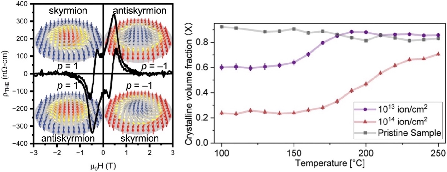
Structural Properties & Recrystallization Effects in Ion Beam-Modified FeGe Thin Films
PARADIM researchers explore tunable disorder in epitaxial FeGe (B20) films to host skyrmions and antiskyrmions. Ion irradiation creates crystalline–amorphous regions; subsequent in situ annealing alters crystalline volume fraction per Johnson–Mehl–Avrami–Kolmogorov kinetics. This tunable system may enable novel spintronic magnetic textures and devices.
Showing 31 to 40 of 363