
Latest News
Highlight ·
Pennsylvania State University
Orientation control of epitaxial transition metal dichalcogenides on hexagonal boron nitride via defects
In two recent 2DCC publications, joint experimental and theory efforts identified a general method to achieve orientational selectivity, originating from a localized defect pair that amplifies the energetic distinction between the two orientations.
Highlight ·
Cornell University
Stretching Valleytronic Materials far beyond Conventional Limits to Tune their Properties
S. Xie, L. Tu, Y. Han, L. Huang, K. Kang, K. U. Lao, P. Poddar, C. Park, D. A. Muller, R. A. DiStasio Jr, J. Park
PARADIM researchers have created superlattice valleytronic materials—still just a single monolayer thick—by modulating the sequence in which the gas precursors are supplied during growth.
Highlight ·
Cornell University
Freeing wafer-scale stacking of single crystals from the shackles of epitaxial constraints
H.S. Kum, H. Lee, S. Kim, S. Lindemann, W. Kong, K. Qiao, P. Chen, J. Irwin, J.H. Lee, S. Xie, S. Subramanian, J. Shim, S.-H. Bae, C. Choi, L. Ranno, S. Seo, S. Lee, J. Bauer, H. Li, K. Lee, J.A. Robinson, C.A. Ross, D.G. Schlom, M.S. Rzchowski, C.-B. Eom, J. Kim
Through the use of “remote epitaxy”—where graphene separates a growing oxide thin film from its substrate—superb crystallinity is achieved together with the ability to peel off oxide layers and create stacks of multiple high-quality layers assembled in a user-defined sequence. The approach heralds a new platform for the limitless stacking of any material into any heterostructure.
Highlight ·
Cornell University
PARADIM machine learning model for assisted optical floating zone synthesis
D. Elbert, B. Schuster, N. Carey, C. Krill, A. Rachidi, W. Phelan, T. McQueen
PARADIM has deployed the first deep learning model of crystal synthesis to assist facility users as they optimize synthesis conditions and accelerate the realization of their materials design plans.
Highlight ·
Pennsylvania State University
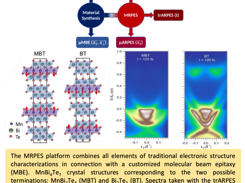
An integrated quantum material testbed with multi-resolution photoemission spectroscopy
Professor Shuolong Yang group at the University of Chicago has set up a new integrated platform for multiresolution photoemission spectroscopy (MRPES) that integrates a helium discharge lamp, a narrow bandwidth 6 eV laser, and a tunable ultrafast laser, which effectively combines static ARPES, time-resolved ARPES (trARPES), and micro-ARPES (μARPES).
Highlight ·
Pennsylvania State University
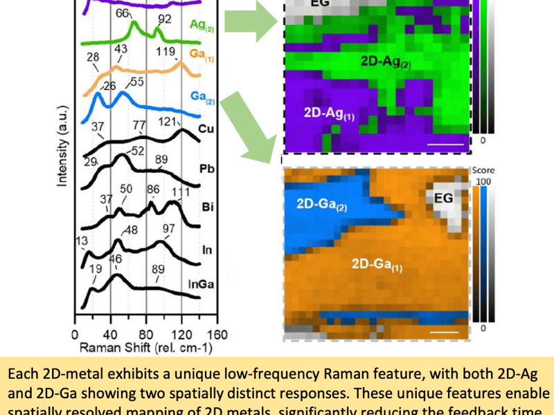
Fingerprinting 2-Dimensional Polar Metals
In this highlight, we identified newly discovered low-frequency (LF) (<100 cm−1 ) Raman features due to the formation of unique 2D polar metals (Ag, Cu, Pb, Bi, Ga, In) or metal alloys (InxGa1−x) intercalated at an epitaxial graphene (EG)/silicon carbide (SiC) interface and demonstrate that 2D-Ag and 2DGa can have spatially distinct phases with their own unique Raman responses. Additionally, we establish that the 2D-Ga exhibits a structural evolution as a function of temperature, independent of the SiC and EG, that can lead to nucleation of secondary phases.
Highlight ·
Cornell University
Quantification of Interfacial Electron-Phonon Coupling from Photoemission Replica Bands in a High-Tc Superconductor
Darrell G. Schlom, Kyle M. Shen
The PARADIM research team has developed a system to transfer sensitive samples from ultrahigh vacuum directly into an inert environment glovebox for transport to the Advance Light Source for beamline ARPES measurements.
Highlight ·
Pennsylvania State University
Dual-sided Adsorption onto 2D
When an atomically thin 2D material is suspended as a membrane so that adsorbed atoms can stick to both sides, these atoms can interact through the membrane and thus act as two coupled adsorbate systems, with new properties that are absent in either system alone. Computational modeling in the 2D Crystal Consortium predicts new patterns that emerge, such as an infinite staircase of fractional coverages of opposing sides with simple rational fractions being favored, a so-called “Devil’s Staircase.”
Highlight ·
Pennsylvania State University
Scalable Substitutional Re-Doping and its Impact on the Optical and Electronic Properties of Tungsten Diselenide
Doping is the cornerstone of semiconductor technology, enabling the success of modern digital electronics. Successful realization of wafer-scale, electronic grade, intrinsic 2D TMDCs via common deposition methods is rapidly progressing, however, advances in scalable doping still remain in the “proof-of-concept” stage, delaying the large-scale fabrication of logic circuits based on extrinsic 2D semiconductors. This work is presenting a wafer-scale synthesis of rhenium doping of WSe2 films via MOCVD at front-end-of-line (FEOL) and back-end-of-line (BEOL) compatible temperatures.
Highlight ·
Pennsylvania State University
Multiphysics Model and Application Development for Controlled 2D Materials Growth
This review provided an overview of theoretical, computational, and machine learning methods and tools at multiple length and time scales, and how they can be utilized to assist/guide the design and synthesis of 2D materials. It focuses on three methods at different length and time scales.
Showing 321 to 330 of 363