Research Highlights
Sep 1, 2025
Cornell University
Fully transparent transistors fabricated at Back-End-of-Line conditions
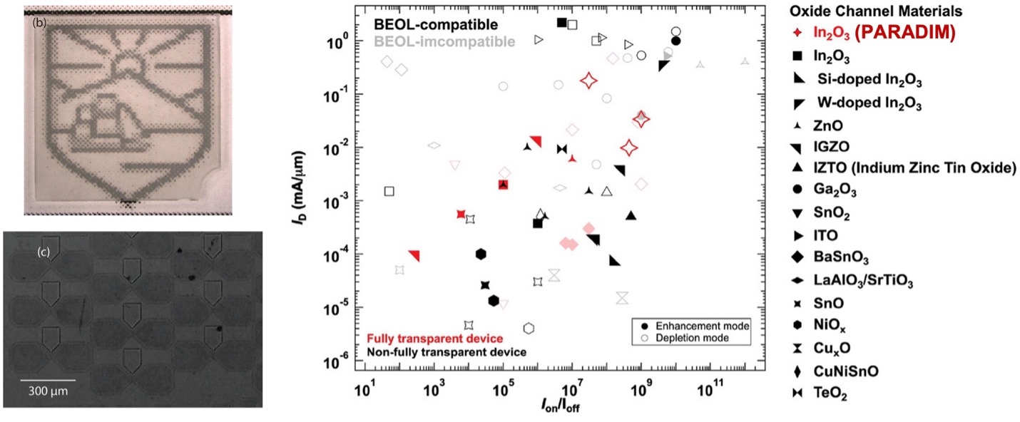
PARADIM’s Highlight #109 reports that suboxide MBE (S-MBE) enables epitaxial In2O3 at BEOL temperatures, yielding the highest-performance fully transparent oxide TFTs to date. The pre-oxidized In2O beam provides exceptional crystal quality and BEOL-compatible devices, accelerating open collaboration and 22 publications across 34 PARADIM projects.
Aug 1, 2025
Cornell University
Growth of hexagonal BN crystals by traveling-solvent floating zone
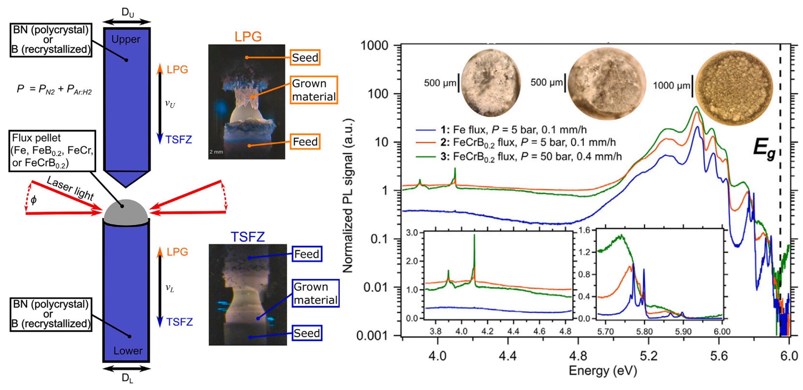
PARADIM Highlight #108 reports scalable growth of high-purity hexagonal boron nitride (h-BN) crystals via solvent laser pedestal and traveling-solvent floating-zone methods, achieving 3–5 mm diameters and multi-mm lengths. This enables larger, defect-minimized h-BN for 2D devices; funded by PARADIM, with collaborators at KU, Texas Tech, Montpellier, UCSB, JHU.
Jun 1, 2025
Cornell University
Structural Properties & Recrystallization Effects in Ion Beam-Modified FeGe Thin Films
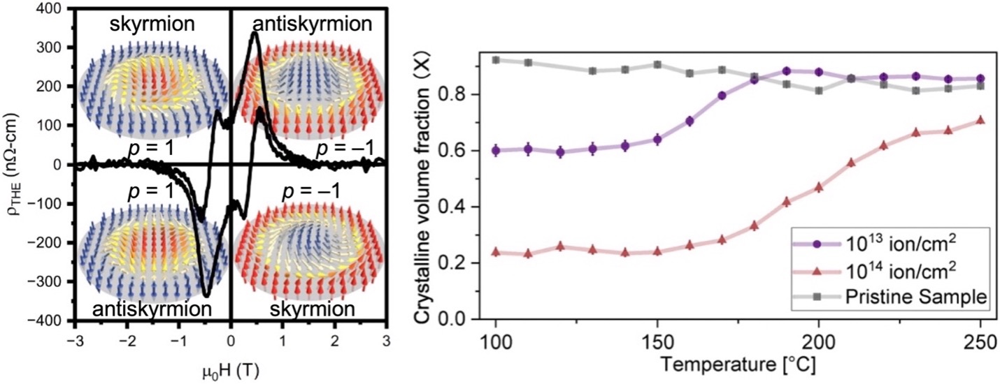
PARADIM researchers explore tunable disorder in epitaxial FeGe (B20) films to host skyrmions and antiskyrmions. Ion irradiation creates crystalline–amorphous regions; subsequent in situ annealing alters crystalline volume fraction per Johnson–Mehl–Avrami–Kolmogorov kinetics. This tunable system may enable novel spintronic magnetic textures and devices.
Jun 1, 2025
Cornell University
Topotactic Ion Intercalation for Designer Magnetic Heterostructures and Devices
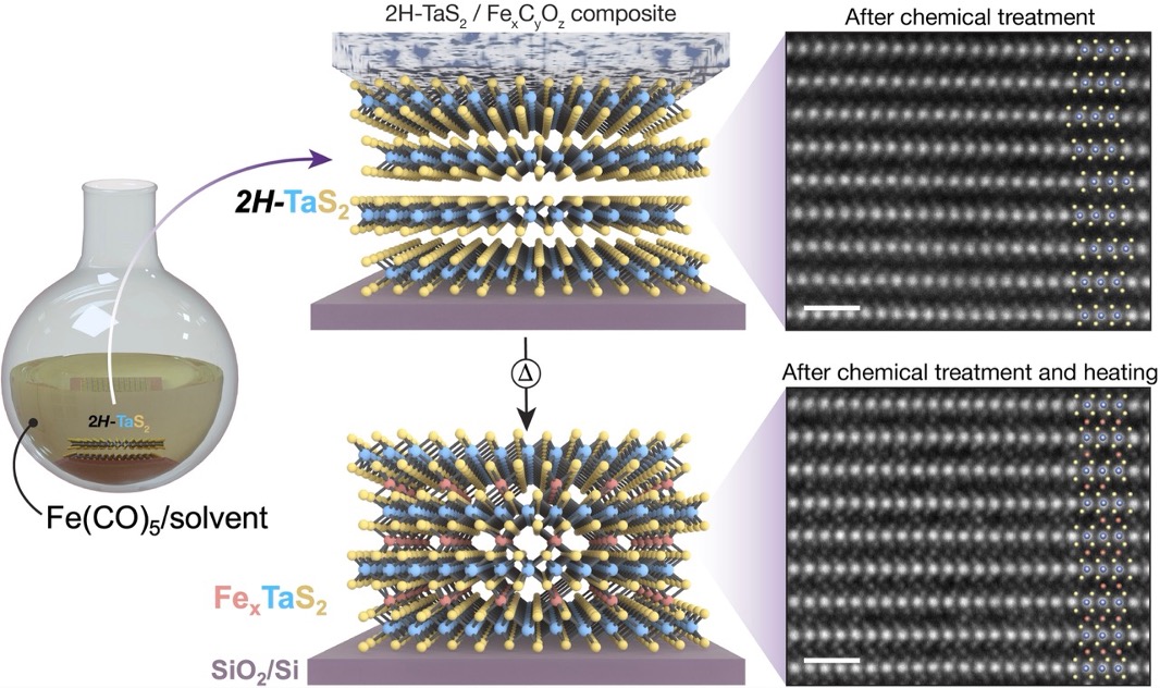
UC Berkeley researchers have developed a method to synthesize magnetic intercalation compounds within transition metal dichalcogenides (TMDs), enhancing the customization of electronic and magnetic device architectures. This approach, utilizing thermal annealing and atomic-resolution imaging, allows for precise control over material properties, opening avenues for advanced spintronic applications.
Jun 1, 2025
Cornell University
Sensing the Local Magnetic Environment in Thin Films
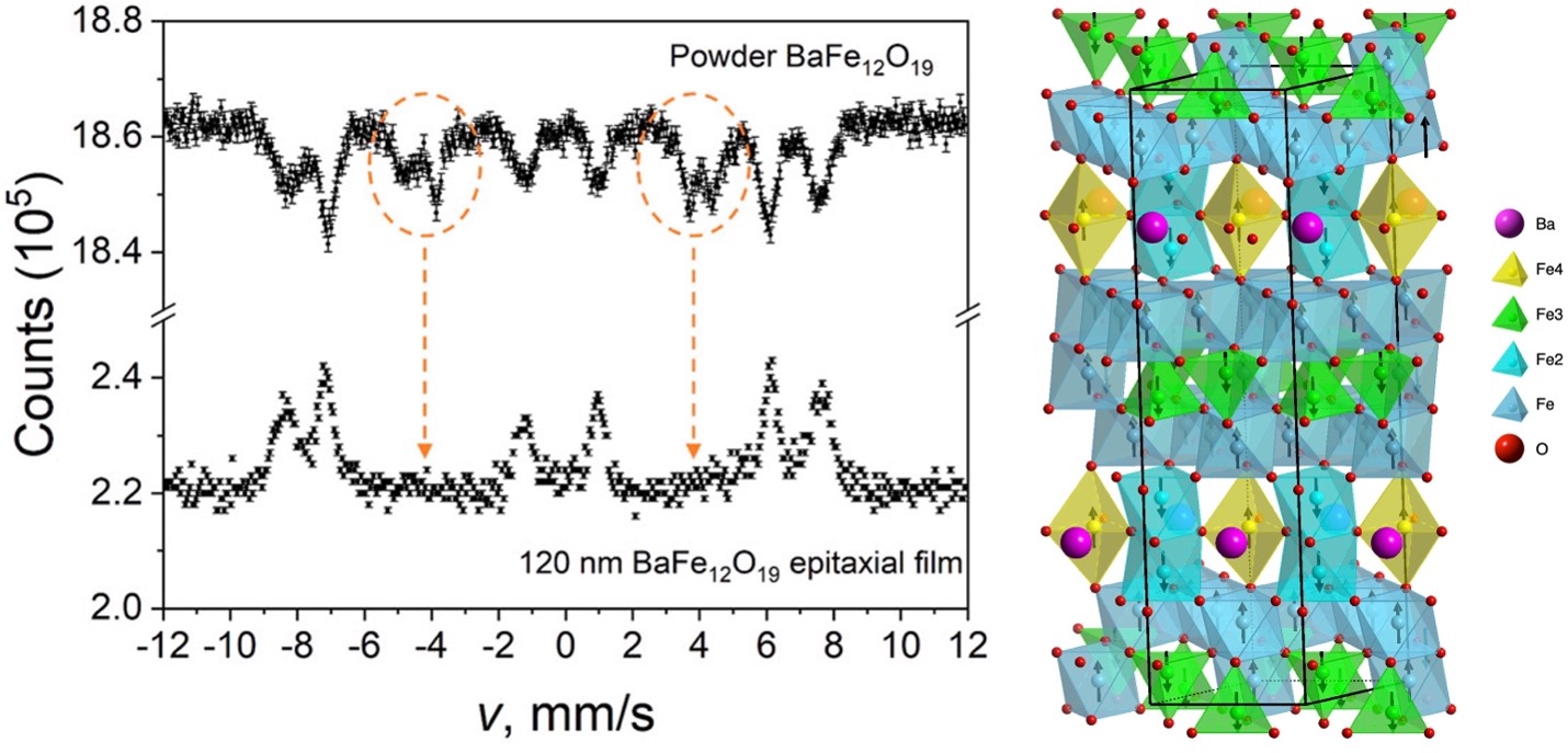
PARADIM Highlight #106 discusses the application of Mössbauer spectroscopy, specifically conversion electron Mössbauer spectroscopy (CEMS), to study thin films of isotopically purified iron. Researchers from Spelman College and Cornell University explored the magnetic orientation of iron in films, demonstrating its utility in analyzing complex magnetic structures.
May 1, 2025
Cornell University
Signatures of Ambient Pressure Superconductivity
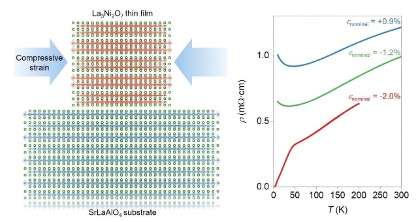
Stanford/SLAC team led by Harold Hwang stabilized ambient-pressure superconductivity in bilayer nickelate La3Ni2O7 thin films using substrate-induced lateral compression, achieving Tc about 26–42 K; defects and oxygen content influence transport. PARADIM EM techniques enabled microstructure insights. This opens routes to studying superconductivity in nickelates at ambient pressure.
May 1, 2025
Cornell University
Experimentally validated Inverse Design of FeNiCrCoCu MPEAs and Unlocking Key Insights with Explainable AI
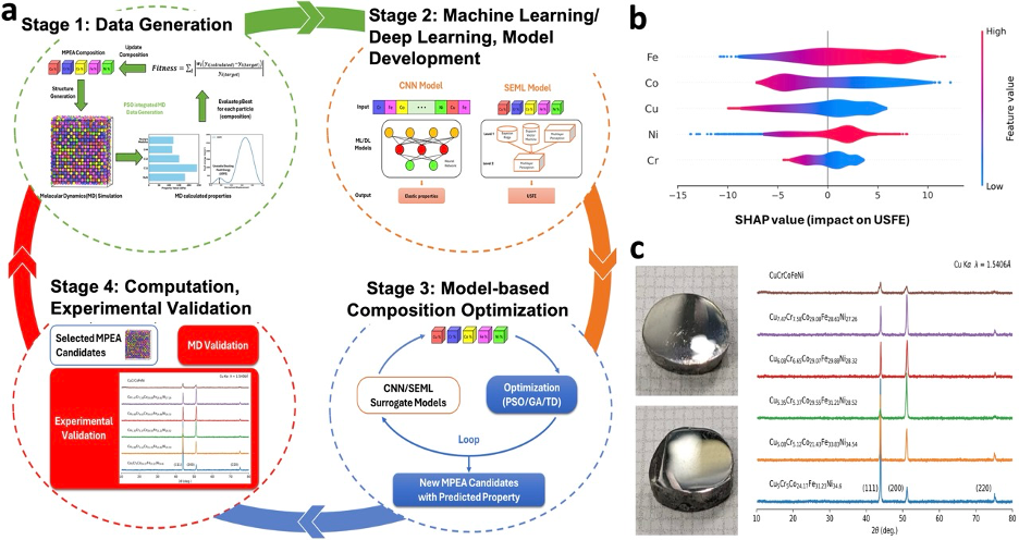
Researchers developed a machine learning-based computational workflow to design FeNiCrCoCu multi-principal element alloys (MPEAs) with improved mechanical properties. Synthesized MPEAs showed experimental validation of predictions. This integrated approach enhances materials design and can be applied to various material systems. Research supported by GlycoMIP and PARADIM.
Apr 1, 2025
Virginia Polytechnic Institute and State University
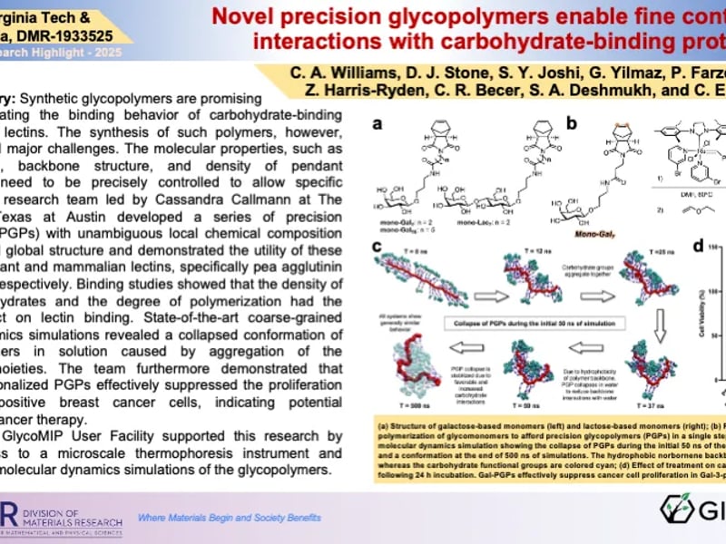
Novel precision glycopolymers enable fine control over interactions with carbohydrate-binding proteins
C. A. Williams, D. J. Stone, S. Y. Joshi, G. Yilmaz, P. Farzeen, S. Jeon, Project summary: Synthetic glycopolymers are promising Z. Harris-Ryden, C. R. Becer, S. A. Deshmukh, and C. E. Callmann
A team of researchers, led by Cassandra Callmann at The University of Texas at Austin, developed a synthesis method for glycopolymers that affords precise control over polymer length, backbone structure, and density of pendant carbohydrates. The team identified the latter to be a critical factor for lectin binding with grafting densities below 50% resulting in weaker interactions.
Apr 1, 2025
Cornell University
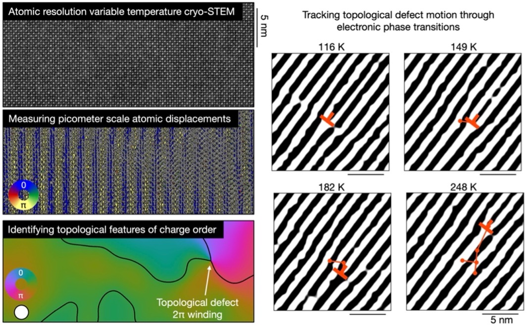
Tracking Topological Defect Motion Through Temperature at the Atomic Scale
PARADIM Highlight #102 reports atomic-resolution tracking of topological defects during the melting of charge-ordered Bi(1−x)Sr(x−y)Ca(y)MnO3 using cryogenic scanning transmission electron microscopy. It reveals defect-network reconfigurations and incommensurate charge order, offering nanoscale insight into electronic phase transitions with relevance to superconductivity and quantum materials.
Apr 1, 2025
Cornell University
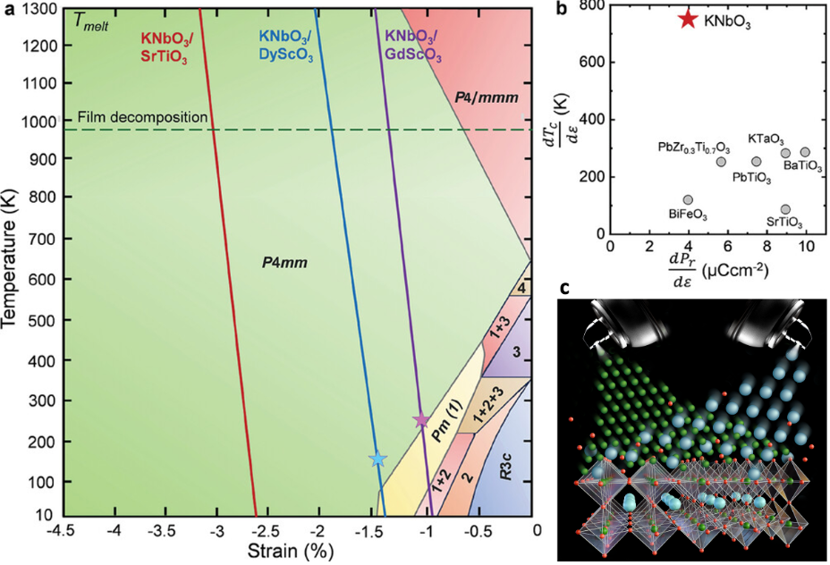
The Right Squeeze: Crafting the Ferro-electric Transitions of KNbO3 Thin Films
PARADIM Highlight #99 reports KNbO3 ferroelectric thin films grown by suboxide molecular-beam epitaxy, showing colossal strain tuning: Tc exceeds 975 K, a single tetragonal phase persists from 10–975 K, polarization up 46%, and second-harmonic generation up ~200%. Lead-free material with high-temperature ferroelectric potential.
Showing 11 to 20 of 237