Research Highlights
Growth of Stoichiometric B4C Single Crystal by Laser Floating-Zone Method
Introduction:
Boron carbide (B4C) is an extremely hard material with a melting temperature above 2000°C; its electronic properties vary strongly with the precise composition.
PARADIM’s Tilting Laser Diode Floating Zone Furnace enables users to routinely grow B4C single crystals for further study. The in-situ monitoring of gas-phase species during the growth provides insights on the underlying mechanism by which the composition changes and enables the successful growth of single crystals with controlled stoichiometry. Various growth rates were explored to mitigate microstructure defects (including stacking faults, SF) and zone refinement allowed for a significant reduction of trace impurities. Initial analysis by powder x-ray diffraction confirms that the crystals are indeed rhombohedral B4C, with a hardness of 41±1 GPa and a Young’s modulus of 520±14 GPa revealed by nano-indentation. Laser light was found to induce graphitization in the presence of air, enabling a new process to fabricate electronic structures in boron carbide with micron or nanoscale precision.
M. Straker et al. J. Cryst. Growth 543, 125700 (2020).
M.V.S. Chandrashekhar et al., U.S. Patent No. US20190352234-A1 (21 November 2019).
|
|
|
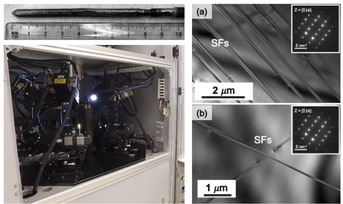
Figure 1: (top left) Photograph of a boron carbide crystal. (bottom left) View into the laser diode floating zone furnace (right) Scanning electron microscopy images of a B4C single crystal with indicated stacking fault lines. |
Technical details: We report the growth of 4 mm diameter × 50 mm long Boron Carbide (B4C) with large single crystal regions using a Laser Diode Floating Zone (LDFZ) method at varying growth rates of 5–20 mm/hr. These materials were grown using polycrystalline B4C as a seed. Microstructural characterization shows the presence of a significant number of twinning-boundaries along the growth direction ([0 0 1]h) oriented in the (1210)h plane. At faster growth rates >10 mm/hr, the crystal orientation was reproducible, suggesting a twin-plane mediated growth mechanism. On the contrary, at slower growth rates <10 mm/hr the crystal orientation was not reproducible, suggesting a critical rate for twin-plane mediated growth to dominate.
Zone refinement of these crystals led to a significant reduction of trace impurities to better than 99.999 wt% purity, at the expense of increased twinning. Powder x-ray diffraction confirms that the bulk is rhombohedral B4C, consistent with the microstructural analysis. The X-ray reciprocal space maps reveal the growth direction to be close to the [001]hdirection, and the corresponding ω-rocking curve width is ~530 arcsec. The rocking curve consisted of 3 distinct peaks, indicating in-plane mosaicism, consistent with the twinning observed. Berkovich nano-indentation of the key (001)h plane showed 41 ± 1 GPa hardness, with a Young’s modulus of 520 ± 14 GPa, comparable to literature reports. In addition, it was discovered that the laser field could induce graphitization of boron carbide in air, a new, previously unknown phenomena that led to a patent application due to the potential uses of the technique in fabricating electronic structures in single crystal boron carbide substrates.
Researchers of Morgan State University initialized and performed the work at the PARADIM Bulk Crystal Growth Facility located at John Hopkins University.
Full references:
Michael Straker, Ankur Chauhan, Mekhola Sinha, W. Adam Phelan, M.V.S. Chandrashekhar, Kevin J. Hemker, Christopher Marvel, and Michael Spencer, “Growth of high purity zone-refined Boron Carbide single crystals by Laser Diode Floating Zone method,” J. Cryst. Growth 543, 125700 (2020).
M.V.S. Chandrashekhar, Joshua Letton, Travis Williams, Abdulganiyu Ajilore, and Michael Spencer “Laser Induced Graphitization of Boron Carbide in Air,” U.S. Patent No. US20190352234-A1 (21 November 2019) https://patents.google.com/patent/US20190352234A1/en.
Return to : User Highlights
Accelerating Materials Discovery by Empowering Users—the MIP Difference
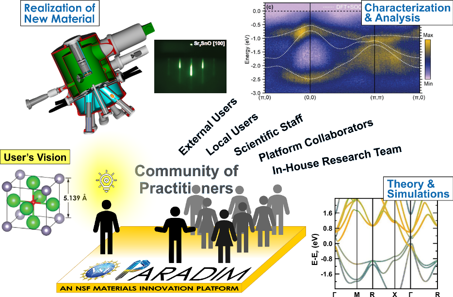
An enlightened and seasoned scientist had a bold vision—to make a new type of topological insulator in a form that could be relevant to technology. The dream compound involved a material predicted to have the desired band structure, but it had never been realized. The group tried for two years to make a simpler version of the material in their own lab, but could not find the right conditions. The group came to PARADIM and in two visits totaling six weeks of round-the-clock molecular-beamtime, they succeeded!
|
|
Figure: Schematic representation of a new user with a brilliant idea of a new type of material boarding the Platform PARADIM. Joining the Community of Practitioners comprised of users, the in-house team, collaborators, and scientific staff, enables close collaborations to accelerate materials discovery by: (i) realization of the material in thin film form using MBE, (ii) characterization and analysis by in situ ARPES and corresponding bandstructure calculations, and (iii) performing required computation in PARADIM's Theory and Simulation facility. |
Guided by thermodynamic calculations from Platform collaborators at Penn State, a growth protocol was designed and implemented on PARADIM’s signature tool that enabled exquisite control of the sample growth. All relevant measurements were made without exposing the sample to air to assess and optimize its crystalline perfection and electronic structure. The bandstructure of the new material was measured and compared to calculated expectations provided by PARADIM’s Theory & Simulation Facility. This new type of topological insulator should be more readily tuned by the underlying substrate and layering to provide desired and technologically useful properties than traditional topological insulators.
What Has Been Achieved: Topological materials are derived from the interplay between symmetry and topology. Advances in topological band theories have led to the prediction that the antiperovskite oxide Sr3SnO is a topological crystalline insulator, a new electronic phase of matter where the conductivity in its (001) crystallographic planes is protected by crystallographic point group symmetries. Realization of this material, however, is challenging. Guided by thermodynamic calculations, a deposition approach is designed and implemented to achieve the adsorption-controlled growth of epitaxial Sr3SnO single-crystal films by molecular-beam epitaxy (MBE). In situ transport and angle-resolved photoemission spectroscopy measurements reveal the metallic and electronic structure of the as-grown samples. Compared with conventional MBE, the “suboxide MBE” synthesis route used results in superior sample quality and is readily adapted to other topological systems with antiperovskite structures.
Importance of the Achievement: This synthesis approach leads to films of exceptional quality enabling the intrinsic non-trivial topology of the correlated electrons in Sr3SnO by ARPES to be established. The fabrication process can be adapted to produce other A3BO-based topological crystalline insulator materials, which will significantly expand the materials space for topological crystalline insulator research and foster the engineering of topological electronics.
Unique Feature(s) of the MIP that Enabled this Achievement: Realizing this challenging material was made possible by PARADIM’s community of practitioners pulling together to collaboratively identify a synthesis path and making use of a signature tool that combines MBE, ARPES, XPS, LEED, R vs. T and electronic property calculations. This material is unstable in air, so the extensive in situ measurements possible in PARADIM were essential in creating this material and comparing its optimized properties with theoretical predictions.
The work was conceived and performed by PARADIM users from the University of Wisconsin-Madison and with contributions from Penn State University, supported by PARADIM staff scientists and members of PARADIM’s In-House Research Team.
Full Reference: Y. Ma, A. Edgeton, H. Paik, B. Faeth, C. Parzyck, B. Pamuk, S.-L. Shang, Z.-K. Liu, K.M. Shen, D.G. Schlom, and C.-B. Eom, “Realization of Epitaxial Thin Films of the Topological Crystalline Insulator Sr3SnO,” Adv. Mater. 32, 2000809 (2020).
Data Reference: Experimental raw data are available at https://data.paradim.org/113.
PARADIM accelerates discovery of nanoscale chemical gradients in human enamel crystallites
New Sample Holder for High-Resolution Electron Microscopy at Previously Inaccessible Temperatures
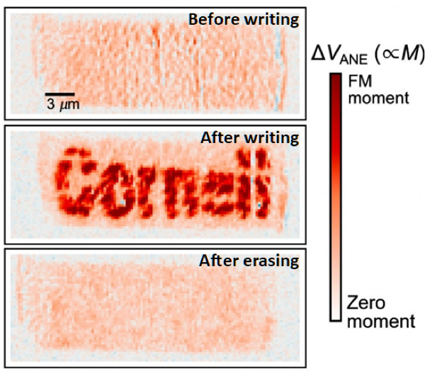
Materials Enabling a Magnetic “Midas Touch”
A Strategy to Make and Manipulate Magnetic Monopoles by Exploiting Interfaces
Ludi Miao, Yonghun Lee, Antonio B. Mei, Michael J. Lawler, Kyle M. Shen
New theoretical approach to tackle interface quantum materials
E. Gerber, Y. Yao, T.A. Arias, E.-A. Kim
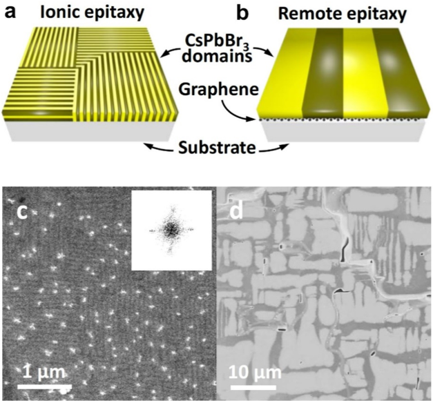
Mollifying Barriers to Enhance Self Assembly
Theory + MBE + ARPES to navigate correlated materials
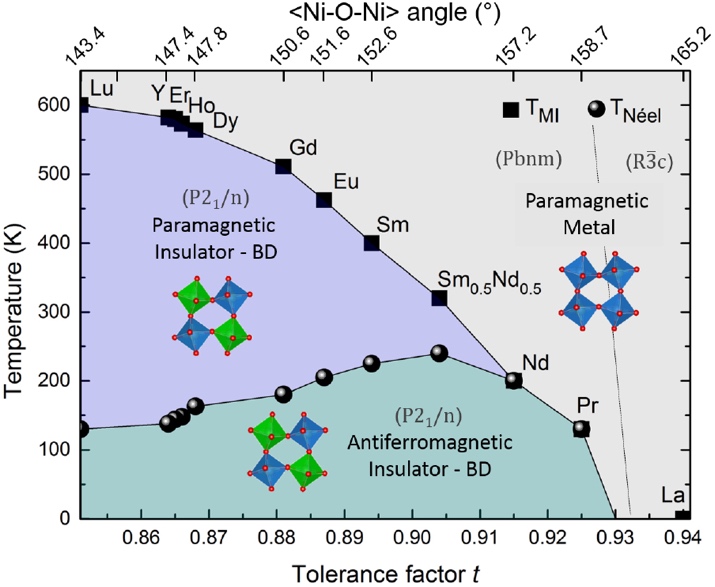
Floating Zone Crystal Growth at Record Oxygen Pressure to Create a PrNiO3 Single Crystal
Showing 141 to 150 of 237