
Latest News

News · Jul 1, 2021
Cornell University
David Muller Awarded 2021 Ernst Ruska Prize for Advances in Electron Microscopy
By PARADIM News
The Director of the PARADIM Electron Microscopy Facility, David Muller awarded the Ernst Ruska Prize from The German Society for Electron Microscopy
Highlight · Jun 30, 2021
Cornell University
Quantification of Interfacial Electron-Phonon Coupling from Photoemission Replica Bands in a High-Tc Superconductor
The observation of replica bands by angle-resolved photoemission spectroscopy enables the study of electron-phonon coupling at low carrier densities, particularly in monolayer FeSe/SrTiO3. Theoretical work suggests that the electrons in the ultra-thin FeSe layer couple to optical phonons in the SrTiO3 substrate that thereby contributes to the enhanced superconducting pairing temperature. So far, the inherent fragility of such single-layer thick materials and the weak intensity of replica features has limited the quantitative evaluation of their nature.
Highlight · Jun 25, 2021
Cornell University
PARADIM – an Incubator for Collaborations
Important applications like ultrashort pulsed lasers, sensors, laser amplifiers, and digital optical information processing, depend on materials with nonlinear optical properties—that is the material’s nonlinear interaction with electromagnetic waves, :e.g.:, light.
Highlight · Jun 18, 2021
Cornell University
Cryo-STEM Unveils Electronic Order at the Atomic Scale
Lena F. Kourkoutis, Elisabeth A. Nowadnick, Harold Y. Hwang
In quantum materials, electrons can interact strongly with each other and with the atomic lattice, giving rise to novel electronic states with functionalities not achievable in conventional materials. At the atomic scale, the local crystal symmetries are governed by variations in the charge distribution and subtle atomic displacements, dramatically affecting the material’s properties.
Highlight · Jun 10, 2021
Cornell University
Discovery of “Pseudogap” Behavior in a Monolayer Thick High-Temperature Superconductor
Darrell G. Schlom, Kyle M. Shen
Members of PARADIM’s in-house research team have employed a combination of angle-resolved photoemission spectroscopy and in situ resistivity measurements to simultaneously probe both the electronic states and superconducting behavior of pristine monolayer FeSe/SrTiO3.
Highlight · Jun 10, 2021
Cornell University
Discovery of “Pseudogap” Behavior in a Monolayer Thick High-Temperature Superconductor
The ability to produce pristine atomic interfaces by growing the structures atom-by-atom :via: molecular beam epitaxy has opened the door to an entirely new class of emergent phenomena in the form of interface quantum materials. One remarkable example of such a material system is the interface between monolayer iron selenide (FeSe) films and SrTiO:3:, where superconductivity can be observed at dramatically higher temperatures compared to 8 K of bulk FeSe. So far, the inherent fragility of such ultra-thin layers has prevented the direct study of superconductivity :via: direct probes like electrical resistivity.

News · Jun 4, 2021
NSF Continues Support for Inaugural Materials Innovation Platforms
The U.S. National Science Foundation funds fundamental research to enhance U.S. competitiveness, economy, and people's lives. The Materials Innovation Platforms (MIPs) program was initiated in 2015 in response to national needs in mid-scale research infrastructure for accelerating materials research. "Materials Innovations Platforms represent a new modality for supporting scientific research," says Linda Sapochak, director of the Division of Materials Research at NSF. "The MIP program provides the required infrastructure made available to a diverse set of stakeholders to support transdisciplinary research and training, to provide broad access to cutting-edge tools, and to facilitate data and knowledge sharing in key enabling areas of national priority."
Highlight · Jun 3, 2021
Cornell University
Remote Epitaxy of 3D functional semiconductors and oxides using Graphene as the Interface layer
H. Paik:, :S. Xie:, H. Shin, C. Choi, J.H. Le, :C. Dong:, :J.A. Robinson (2DCC):, :J.-H. Lee:, J.-H. Ahn, G.Y. Yeom, :D.G. Schlom (PARADIM):, J. Kim (MIT):Project Summary::Remote epitaxy has drawn attention as it offers epitaxy of functional materials that can be released from the substrates with atomic precision, thus enabling production and heterointegration of flexible, transferrable, and stackable freestanding single-crystalline membranes. In this highlight, 2DCC and PARADIM team up to work with the inventor of remote epitaxy, Prof. Kim (MIT), to unveil the respective roles and impacts of the substrate material, graphene, substrate–graphene interface, and epitaxial material for electrostatic coupling of these materials, which governs cohesive ordering and can lead to single-crystal epitaxy in the overlying film.
Highlight · May 31, 2021
University of California, Santa Barbara
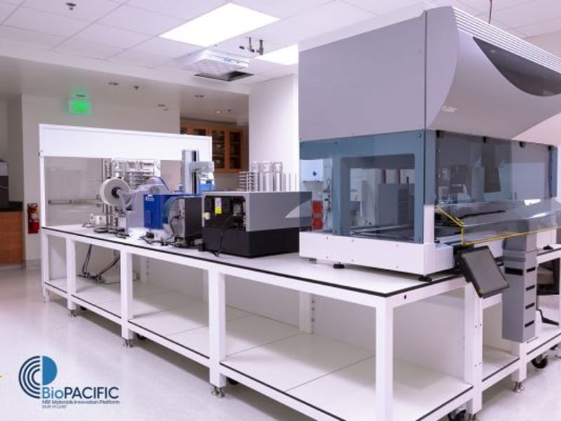
Living Biofoundry Becomes Available
The BioPACIFIC MIP Living Biofoundry (LBF) has been installed at UCLA and is now available to users.

News · May 31, 2021
University of California, Santa Barbara
Living Biofoundry Brings New Synthetic Biology and Microbial Engineering Capabilities to BioPACIFIC MIP
UCLA's BioPACIFIC Materials Innovation Platform has launched the Living Biofoundry, a shared resource for researchers developing microbes for sustainable materials. This NSF-funded facility features advanced automation systems for high-throughput synthetic biology, aiding the production of bioderived polymers and chemicals. Access is open to U.S. scientists via a peer-reviewed proposal process.
Showing 211 to 220 of 363