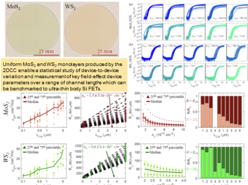
To assess the potential of transition metal dichalcogenides (MDs) for future circuits, it is important to study the variation in key device parameters across a large number of devices. Here we benchmark device-to-device variation in field- effect transistors (FETs) based on wafer-scale monolayer MoS, and WS. Our study involves 230 MoS, FETs and 160 WS, FETS with channel lengths ranging from 5 um down to 100 nm. We use statistical measures to evaluate key FET performance indicators for benchmarking these MD monolayers against existing literature as well as ultra-thin body Si FETs. Our results show consistent performance of the 2D FETs across 1×1 cm? chips owing to high quality uniform layers and clean transfer onto device substrates. We demonstrate record high carrier mobility of 33 cm?V-is-1 in WS, FETs, which is a 1.5X improvement compared to the best literature report Our results confirm the technological viability of 2D FETs in future integrated circuits Published in Nature Communications 2021, 12, 1-12.
 Download

2D Crystal Consortium - Materials Innovation Platform (2DCC-MIP)
The 2DCC-MIP combines a vibrant in-house research effort focused on transformative advances in the synthesis and characterization of 2D chalcogenide layered materials with a robust external user program that provides access to expertise and state-of-the-art facilities. The 2DCC-MIP platform enables cutting edge research and discovery, across in-house research and the user program, on the synthesis and characterization of 2D chalcogenide materials by a national user community guided by four science drivers: Physics of 2D Systems, Epitaxy of 2D Chalcogenides, Next-generation 2D Electronics, and Advanced Characterization and Modeling.