Benchmarking monolayer MoS, and W, field-effect transistors

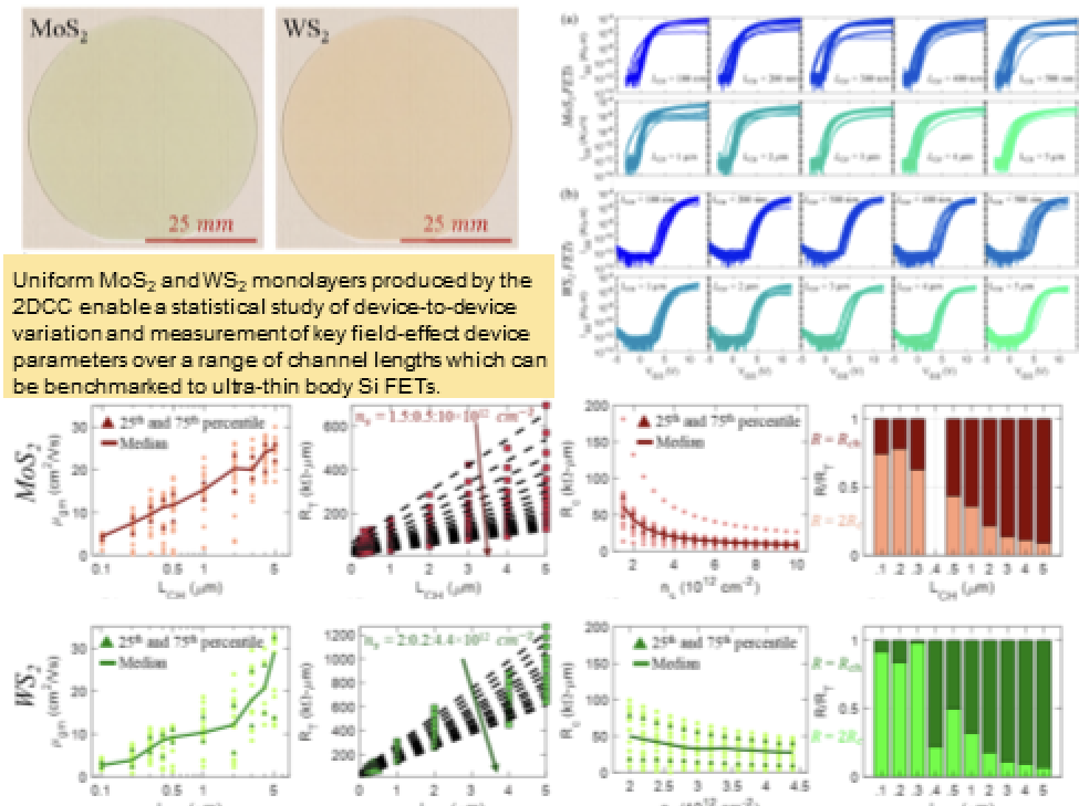
To assess the potential of transition metal dichalcogenides (MDs) for future circuits, it is important to study the variation in key device parameters across a large number of devices. Here we benchmark device-to-device variation in field- effect transistors (FETs) based on wafer-scale monolayer MoS, and WS. Our study involves 230 MoS, FETs and 160 WS, FETS with channel lengths ranging from 5 um down to 100 nm. We use statistical measures to evaluate key FET performance indicators for benchmarking these MD monolayers against existing literature as well as ultra-thin body Si FETs. Our results show consistent performance of the 2D FETs across 1×1 cm? chips owing to high quality uniform layers and clean transfer onto device substrates. We demonstrate record high carrier mobility of 33 cm?V-is-1 in WS, FETs, which is a 1.5X improvement compared to the best literature report Our results confirm the technological viability of 2D FETs in future integrated circuits Published in Nature Communications 2021, 12, 1-12.
CONTACT:
National Science Foundation
Division of Materials Research
2415 Eisenhower Avenue
Alexandria, VA 22314

Any opinions, findings and conclusions or recommendations expressed in this material are those of the author(s) and do not necessarily reflect the views of the National Science Foundation.
SOCIAL: