Suboxide Molecular-Beam Epitaxy—Translating a new Concept into β-Ga2O3 Transistors
APL Materials
PARADIM Highlight #80
In 2020 PARADIM’s in-house team—working with collaborators at Penn State—developed (and patented) a new variant of molecular-beam epitaxy (MBE) called “suboxide MBE.” In contrast to conventional MBE where the molecular beams are elemental, in suboxide MBE the molecular beams are pre-oxidized. This method has since been widely applied by PARADIM users in 20 publications utilizing suboxide MBE + over 20 active user projects).
A recent publication from a team of PARADIM users:
Local users (film growth, XRD, AFM, Hall effect, STEM)
In-House (film growth, XRD, Hall effect)
PARADIM PREM (SIMS)
Air Force Research Lab (transistor fabrication + testing)
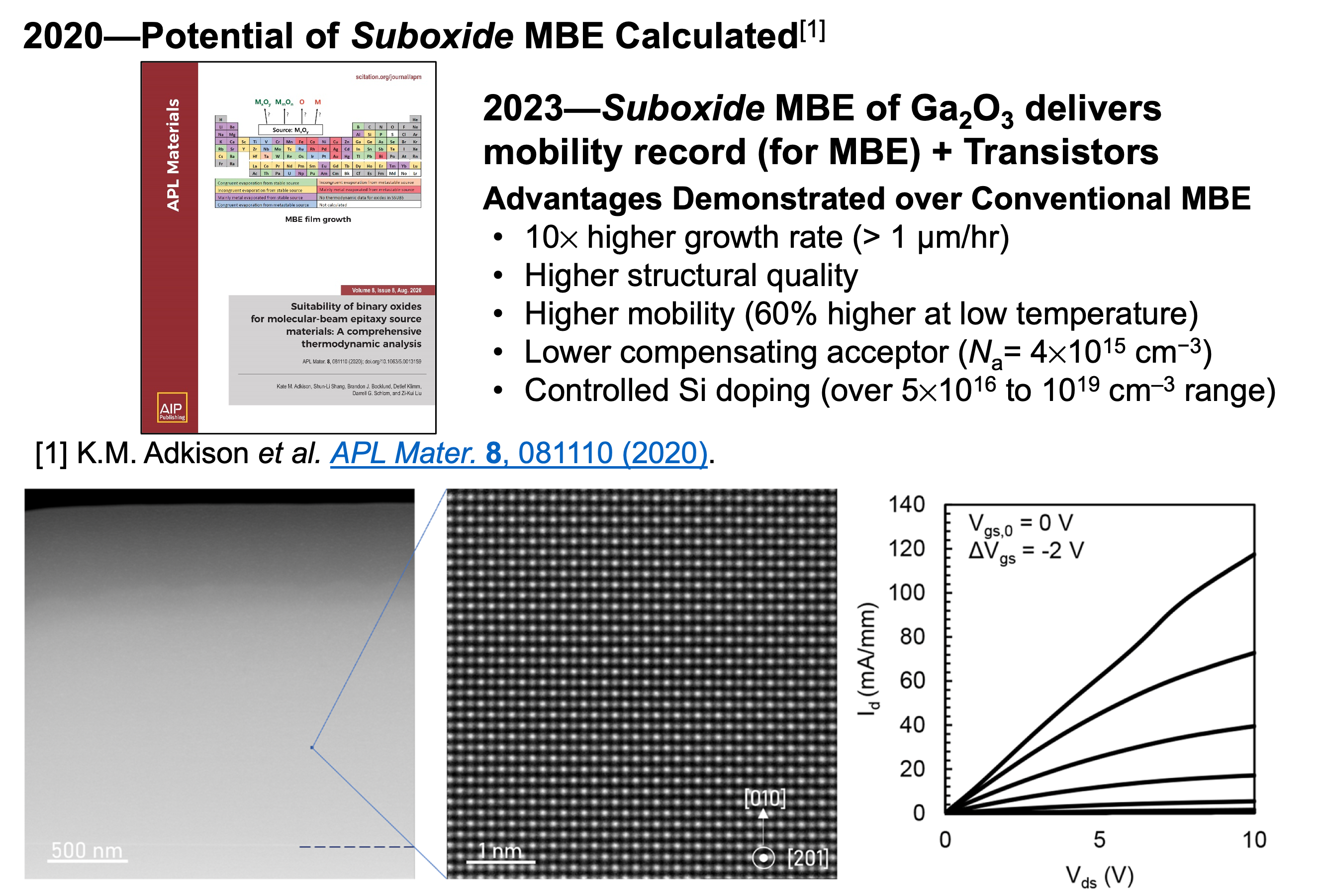
demonstrates its promise for the growth of transistors of the high-bandgap semiconductor b-Ga2O3. Suboxide MBE produced device-quality films with lots of advantages over conventional MBE including new records in lower background impurity levels and higher low-temperature mobility, despite the 10✕ higher growth rate and superb structural quality.
What has been achieved:
We report the use of suboxide molecular-beam epitaxy (S-MBE) to grow β-Ga2O3 at a growth rate of ∼1 μm/h with control of the silicon doping concentration from 5 × 10¹⁶ to 1019 cm−3. In S-MBE, pre-oxidized gallium in the form of a molecular beam that is 99.98% Ga2O, i.e., gallium suboxide, is supplied. Directly supplying Ga2O to the growth surface bypasses the rate-limiting first step of the two-step reaction mechanism involved in the growth of β-Ga2O3 by conventional MBE. As a result, a growth rate of ∼1 μm/h is readily achieved at a relatively low growth temperature (Tsub ≈ 525 °C), resulting in films with high structural perfection and smooth surfaces (rms roughness of <2 nm on ∼1 μm thick films). Silicon-containing oxide sources (SiO and SiO2) producing an SiO suboxide molecular beam are used to dope the β-Ga2O3 layers. Temperature-dependent Hall effect measurements on a 1 μm thick film with a mobile carrier concentration of 2.7 × 1017 cm−3 reveal a room-temperature mobility of 124 cm2 V−1 s−1 that increases to 627 cm2 V−1 s−1 at 76 K; the silicon dopants are found to exhibit an activation energy of 27 meV. We also demonstrate working metal–semiconductor field-effect transistors made from these silicon-doped β-Ga2O3 films grown by S-MBE at growth rates of ∼1 μm/h.
[1] K.M. Adkison, S.-L. Shang, B.J. Bocklund, D. Klimm, D.G. Schlom, and Z.-K. Liu, "Suitability of Binary Oxides for Molecular-Beam Epitaxy Source Materials: A Comprehensive Thermodynamic Analysis," APL Mater. 8, 081110 (2020), DOI 10.1063/5.0013159—a PARADIM publication selected as journal cover for APL Materials, Issue August 2020.
Importance of the Achievement:
Suboxide MBE is a new variant of MBE that provides advantages for the synthesis of many oxygen-containing compounds. This MBE variant was invented (and patented) by PARADIM’s In-House team working with Prof. Zi-Kui Liu at Penn State, who performed the comprehensive thermodynamic calculations for binary oxides of the entire periodic table—128 binary oxides in all—plus an additional 27 two-phase mixtures of binary oxides with their elements. These calculations established the promise of this approach, at least from a thermodynamic perspective. This method has been widely applied by PARADIM users in 20 publications utilizing suboxide MBE (see full list below) + over 20 active user projects. Part of the accelerated adoption of this technique arose from knowledge sharing of details of the emerging method before it was published (see Highlight #38). Suboxide MBE has enabled never-before synthesized epitaxial films of Sn2+ materials to be realized, BaSnO3 films to be grown with the highest mobility in the world, VO2 films with ultra-sharp metal-insulator-transitions, and additional challenging electronic materials never before grown by MBE (e.g., KTaO3) to be grown with high quality. Here just 3 years after this initial publication explaining the method, a team of PARADIM users (local users, in-house users, PARADIM-PREM users, and collaborators from the Air Force Research Lab) has translated this discovery in synthesis science to make working devices (transistors) based on the high-bandgap semiconductor β-Ga2O3. The resulting films are not only grown 10x faster than prior MBE-grown β-Ga2O3 with high mobility, but have 60% higher mobility at low temperature and lower concentrations of compensating acceptors. Further, the suboxide MBE approach has enabled controlled doping of the epitaxial layers by MBE over a concentration range relevant to devices. These advances are all key to the fabrication of transistors by the members of this research team at the Air Force Research Laboratory.
PARADIM publications (to date) making use of suboxide MBE in addition to the one highlighted:
T. Schwaigert, S. Salmani-Razaie, M.R. Barone, H. Paik, E. Ray, M.D. Williams, D.A. Muller, D.G. Schlom, and K. Ahadi, "Molecular Beam Epitaxy of KTaO3," J. Vac. Science & Technol. A 41, 022703 (2023).
F.V.E. Hensling, M.A. Smeaton, V. Show, K. Azizie, M.R. Barone, L.F. Kourkoutis, and D.G. Schlom, "Epitaxial growth of the first two members of the Ban+1InnO2.5n+1 Ruddlesden–Popper homologous series," J. Vac. Science & Technol. A 40, 062707 (2022).
P. Vogt, F.V.E. Hensling, K. Azizie, J.P. McCandless, J. Park, K. DeLello, D.A. Muller, H.G. Xing, D. Jena, and D.G. Schlom, "Extending the Kinetic and Thermodynamic Limits of Molecular-Beam Epitaxy Utilizing Suboxide Sources or Metal-Oxide Catalyzed Epitaxy," Phys. Rev. Appl. 17, 034021 (2022).
K. Eom, H. Paik, J. Seo, N. Campbell, E.Y. Tsymbal, S.H. Oh, M. Rzchowski, D.G. Schlom, and C.-B. Eom, "Oxide Two-Dimensional Electron Gas with High Mobility at Room-Temperature," Adv. Sci. 9, 2105652 (2022).
M. Barone, M. Foody, Y. Hu, J. Sun, B. Frye, S.S. Perera, B. Subedi, H. Paik, J. Hollin, M. Jeong, K. Lee, C.H. Winter, N.J. Podraza, K. Cho, A. Hock, and D.G. Schlom, "Growth of Ta2SnO6 Films, a Candidate Wide-Band-Gap p-Type Oxide," J. Phys. Chem. C 126, 3764–3775 (2022).
J. Sun, C.T. Parzyck, J.H. Lee, C.M. Brooks, L.F. Kourkoutis, X. Ke, R. Misra, J. Schubert, F.V. Hensling, M.R. Barone, Z. Wang, M.E. Holtz, N.J. Schreiber, Q. Song, H. Paik, T. Heeg, D.A. Muller, K.M. Shen, and D.G. Schlom, "Canonical Approach to Cation Flux Calibration in Oxide Molecular-Beam Epitaxy," Phys. Rev. Mater. 6, 033802 (2022).
M. Barone, C. Du, L. Radosavljevic, D. Werder, X. Pan, and D.G. Schlom, "Epitaxial Synthesis of a Vertically Aligned Two-Dimensional van der Waals Crystal: (110)-Oriented SnO," Cryst. Growth Des. 22, 7248-7254 (2022).
F.V.E. Hensling, D. Dahliah, P. Dulal, P. Singleton, J. Sun, J. Schubert, H. Paik, I. Subedi, B. Subedi, G.-M. Rignanese, N.J. Podraza, G. Hautier, and D.G. Schlom, "Epitaxial Stannate Pyrochlore Thin Films: Limitations of Cation Stoichiometry and Electron Doping," APL Mater. 9, 051113 (2021).
P. Vogt, F.V.E. Hensling, K. Azizie, C.S. Chang, D. Turner, J. Park, J.P. McCandless, H. Paik, B.J. Bocklund, G. Hoffman, O. Bierwagen, D. Jena, H.G. Xing, S. Mou, D.A. Muller, S.-L. Shang, Z.-K. Liu, and D.G. Schlom, "Adsorption-controlled growth of Ga2O3 by suboxide molecular-beam epitaxy," APL Mater. 9, 031101 (2021).
S. Chae, K.A. Mengle, K. Bushick, J. Lee, N. Sanders, Z. Deng, Z. Mi, P.F.P. Poudeu, H. Paik, J.T. Heron, and E. Kioupakis, "Perspective: Towards the Predictive Discovery of Ambipolarly Dopable Ultra-Wide-Band-Gap Semiconductors: The Case of Rutile GeO2," Appl. Phys. Lett. 118, 260501 (2021).
K.M. Adkison, S.-L. Shang, B.J. Bocklund, D. Klimm, D.G. Schlom, and Z.-K. Liu, "Suitability of Binary Oxides for Molecular-Beam Epitaxy Source Materials: A Comprehensive Thermodynamic Analysis," APL Mater. 8, 081110 (2020).
Y. Ma, A. Edgeton, H. Paik, B. Faeth, C. Parzyck, B. Pamuk, S.-L. Shang, Z.-K. Liu, K.M. Shen, D.G. Schlom, and C.-B. Eom, “Realization of Epitaxial Thin Films of the Topological Crystalline Insulator Sr3SnO,” Adv. Mater. 32, 2000809 (2020).
J. Park, H. Paik, K. Nomoto, K. Lee, B.-E. Park, B. Grisafe, L.-C. Wang, S. Salahuddin, S. Datta, Y. Kim, D. Jena, H. G. Xing, and D. G. Schlom, “Fully Transparent Field-Effect Transistor with High Drain Current and On/Off Ratio,” APL Mater. 8, 011110 (2020).
S. Chae, H. Paik, N.M. Vu, E. Kioupakis, and J.T. Heron, “Epitaxial Stabilization of Rutile Germanium Oxide Thin Film by Molecular Beam Epitaxy,” Appl. Phys. Lett. 117, 072105 (2020).
A.B. Mei, L. Miao, M.J. Wahila, G. Khalsa, Z. Wang, M. Barone, N.J. Schreiber, L.E. Noskin, H. Paik, T.E. Tiwald, Q. Zheng, R.T. Haasch, D.G. Sangiovanni, L.F.J. Piper, and D.G. Schlom, “Adsorption-Controlled Growth and Properties of Epitaxial SnO films,” Phys. Rev. Mater. 3, 105202 (2019).
A. Galdi, C.M. Pierce, L. Cultrera, G. Adhikari, W.A. Schroeder, H. Paik, D.G. Schlom, J.K. Nangoi, T.A. Arias, E. Lochocki, C. Parzyck, K.M. Shen, J.M. Maxson, and I.V. Bazarov “Low Energy Photoemission From (100) Ba1‑xLaxSnO3 Thin Films for Photocathode Applications,” Eur. Phys. J. Spec. Top. 228, 713–718 (2019).
Z. Wang, H. Paik, Z. Chen, D.A. Muller, and D.G. Schlom, “Epitaxial Integration of High-Mobility La-Doped BaSnO3 Thin Films with Silicon,” APL Mater. 7, 022520 (2019).
E.B. Lochocki, H. Paik, M. Uchida, D.G. Schlom, and K.M. Shen, “Controlling Surface Carrier Density by Illumination in the Transparent Conductor La-doped BaSnO3,” Appl. Phys. Lett. 112, 181603 (2018).
H. Paik, Z. Chen, E. Lochocki, A. Seidner H, A. Verma, N. Tanen, J. Park, M. Uchida, S. Shang, B.-C. Zhou, M. Brützam, R. Uecker, Z.-K. Liu, D. Jena, K. M. Shen, D. A. Muller, and D. G. Schlom, “Adsorption-Controlled Growth of La-doped BaSnO3 by Molecular-Beam Epitaxy,” APL Mater. 5, 116107 (2017).
Unique Feature(s) of the MIP that Enabled this Achievement:
It took PARADIM’s In-House team working with a collaborator of the Platform 3 years to develop the comprehensive thermodynamic understanding underlying suboxide MBE. That itself is not unusual. What is unusual, at least from the traditional means of informing others through publication, is that PARADIM began openly sharing the concept of suboxide MBE and preliminary thermodynamic calculations with its users over 2 years prior to publication. This is part of the brainstorming that occurs among members of the Platform as they formulate plans to attempt to make new materials. This goes beyond just informing users of what has been done, but actively brainstorming as a team how to approach the synthesis of their specific systems of interest to realize what has never before been achieved. This is a different way of doing business; it demonstrates the power of a MIP.
Full reference:
K. Azizie, F.V.E. Hensling, C.A. Gorsak, Y. Kim, N.A. Pieczulewski, D.M. Dryden, M.K.I. Senevirathna, S. Coye, S-L. Shang, J. Steele, P. Vogt, N.A. Parker, Y.A. Birkhölzer, J.P. McCandless, D. Jena, H.G. Xing, Z.K. Liu, M.D. Williams, A.J. Green, K. Chabak, D.A. Muller, A.T. Neal, S. Mou, M.O. Thompson, H.P. Nair, and D.G. Schlom, “Silicon-Doped β-Ga2O3 Films Grown at 1 μm/h by Suboxide Molecular-Beam Epitaxy,” APL Materials 11, 041102 (2023).
Acknowledgments:
K.A., C.A.G., N.A.P., J.S., J.P.M., D.J., H.G.X., D.A.M., M.O.T., H.P.N., and D.G.S. acknowledge the support from the AFOSR/AFRL ACCESS Center of Excellence under Award No. FA9550-18-1-0529. J.P.M. also acknowledges the support from the National Science Foundation within a Graduate Research Fellowship under Grant No. DGE-1650441. P.V. and Y.A.B. acknowledge the support from ASCENT, one of six centers in JUMP, a Semiconductor Research Corporation (SRC) program sponsored by DARPA. F.V.E.H. acknowledges the support from the Alexander von Humboldt Foundation in the form of a Feodor Lynen fellowship. F.V.E.H. also acknowledges the support from the National Science Foundation (NSF) [Platform for the Accelerated Realization, Analysis and Discovery of Interface Materials (PARADIM)] under Cooperative Agreement No. DMR-1539918. M.D.W., D.A.M., and D.G.S. acknowledge the support from the NSF under DMR-2122147. M.D.W. also acknowledges NSF Grant No. HRD-1924204 and ONR Award No. N00014-21-1-2823. This work made use of the Cornell Center for Materials Research (CCMR) Shared Facilities, which are supported through the NSF MRSEC Program (Grant No. DMR-1719875). The substrate preparation was performed, in part, at the Cornell NanoScale Facility, a member of the National Nanotechnology Coordinated Infrastructure (NNCI), which is supported by the NSF (Grant No. NNCI-2025233). This work also made use of the Cornell Energy Systems Institute Shared Facilities partly sponsored by the NSF (Grant No. MRI DMR-1338010).