When Seemingly Passive Substrates are Active
featured research
Substrates traditionally play a supporting role for the thin films grown upon them by providing purely structural support. Nonetheless for monolayer-thick transition metal dichalcogenides (TMDs), the substrate plays an active role by providing or removing charge from the TMD layer in which it is in intimate contact. The amount of charge transferred is relatively small (roughly 1013 electrons per square centimeter), but for monolayer-thick materials the addition or subtraction of this amount of charge can have significant doping effects on these materials, making it relevant to the operation of TMD-based electronics. Although charge transfer has been noted by prior researchers investigating TMDs, accurately predicting the charge transfer between TMDs and substrates has been out of reach.
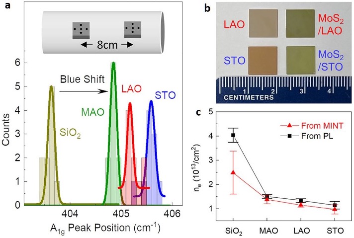
Figure: a) Histograms and their Gaussian fittings of the A1g peak position of MoS2 on different oxide substrates. For each substrate, ten measurements were taken from two samples placed 8 cm apart (inset) during growth of MoS2 in the tube furnace. b) Photograph of monolayer MoS2 grown on 1x1 cm2 LaAlO3 and SrTiO3 substrates. Bare substrates are shown on the left for comparison. c) Comparison of the electron concentration of MoS2 on the four different oxide substrates. Curve one calculated from values based on MINT shows good agreement with curve two derived from experimental photoluminescence measurements.
Thanks to PARADIM’s new first-principles theory—known as mis-matched interface theory (MINT)—this charge transfer can be accurately calculated. PARADIM’s first use of MINT was to calculate the charge transfer between graphene and materials in which it was in contact; the results were in excellent agreement with experiments. Now PARADIM’s in-house team has extended these calculations to TMDs and performed experiments to test the calculations by growing films of the TMD MoS2 on several oxide substrates including SiO2, MgAl2O4, LaAlO3, and SrTiO3. The measured charge transfer is found to be in excellent agreement with the predictions of MINT. The ability to employ a substrate to quantitatively and reproducibly control the doping of a TMD film grown upon it is a powerful addition to the traditional means of controlling the doping through electrostatic gating or the addition of chemical impurities.
What Has Been Achieved:
PARADIM’s in-house research team has demonstrated how by selecting a particular complex oxide substrate, the carrier concentration of a monolayer of MoS2 grown on the substrate exhibits a controlled, reproducible, and uniform carrier concentration ranging from (1–4)x1013 cm-2, depending on the oxide substrate employed. The specific substrates used in this study include perovskite (SrTiO3 and LaAlO3), spinel (MgAl2O4), and SiO2. The multi-inch uniformity of PARADIM’s MOCVD capability is demonstrated by the uniformity in the shifts seen of the A1g Raman peak, sampling across films that were grown at different positions along an 8 cm segment of the MOCVD tube furnace. The observed carrier concentrations are compared to the results of PARADIM’s density-functional theory calculations based on ab initio mismatched interface theory (MINT) and the agreement is seen to be excellent.
Importance of the Achievement:
Bandgap engineering is central to the design of heterojunction devices. For heterojunctions involving monolayer-thick transition metal dichalcogenides (TMD) materials like MoS2, the carrier concentration of the atomically thin film can vary significantly depending on the amount of charge transfer between MoS2 and the substrate. This makes substrates with a range of charge neutrality levels—as is the case for complex oxide substrates—a powerful addition to electrostatic gating or chemical doping to control the doping of overlying MoS2 layers. This approach is relevant to large-scale heterostructures involving monolayer-thick materials in which it is desired to precisely control carrier concentrations for applications. This is a new control knob, where theory can be used to accurately calculate the charge transfer expected for different complex oxide substrates and then a substrate providing the desired charge transfer used to uniformly and reproducibly dope the entire TMD film. This control knob could be used to controllably shift the threshold voltage of transistors built in the overlying TMD film.
Unique Feature(s) of the MIP that Enabled this Achievement:
The Mismatched INterface Theory (MINT) is a product of PARADIM’s in-house research team to accurately describe 2-dimensional materials in contact with other solid materials in a first-principles approach. The versatility of MINT—a tool available to all users of PARADIM—is demonstrated for MoS2 monolayers on single crystal oxide substrates. The excellent uniformity of PARADIM’s MOCVDs for the deposition of MoS2 and other TMDs over large areas allowed the robustness of these results to be demonstrated in this combined theory and experimental study, all by PARADIM’s in-house team.
CONTACT:
National Science Foundation
Division of Materials Research
2415 Eisenhower Avenue
Alexandria, VA 22314

Any opinions, findings and conclusions or recommendations expressed in this material are those of the author(s) and do not necessarily reflect the views of the National Science Foundation.
SOCIAL: