Discovery of “Pseudogap” Behavior in a Monolayer Thick High-Temperature Superconductor

featured research
The ability to produce pristine atomic interfaces by growing the structures atom-by-atom via molecular beam epitaxy has opened the door to an entirely new class of emergent phenomena in the form of interface quantum materials. One remarkable example of such a material system is the interface between monolayer iron selenide (FeSe) films and SrTiO3, where superconductivity can be observed at dramatically higher temperatures compared to 8 K of bulk FeSe. So far, the inherent fragility of such ultra-thin layers has prevented the direct study of superconductivity via direct probes like electrical resistivity.
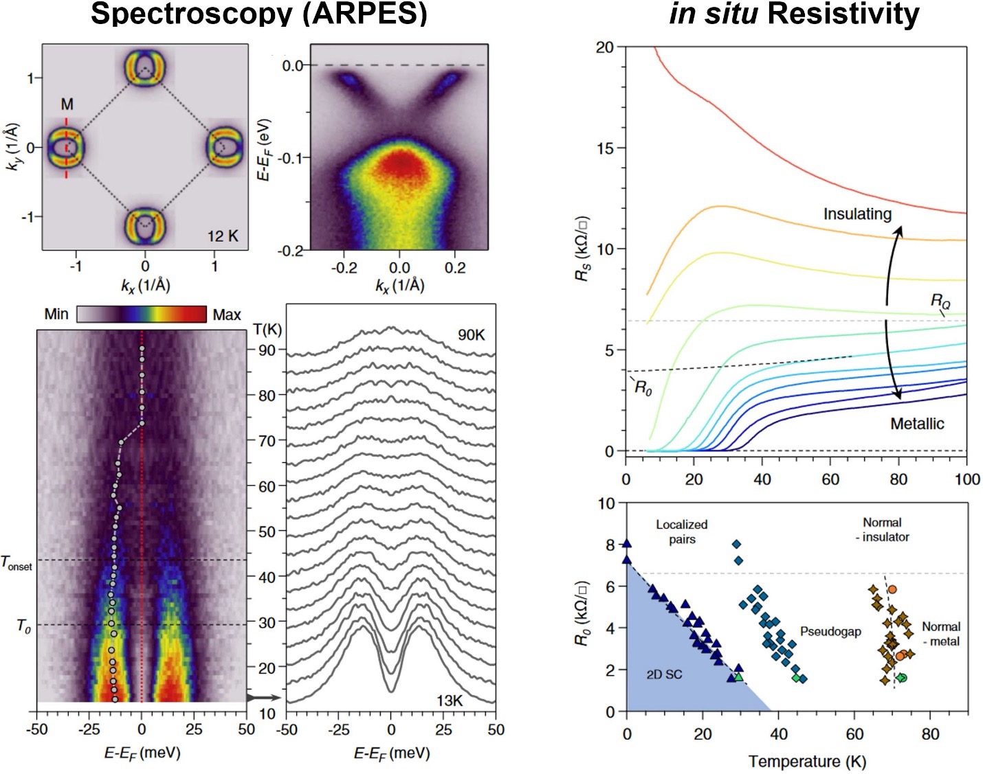
Figure 1: Photoelectron spectroscopy and resistivity analysis of FeSe thin films on SrTiO3. (left top) Fermi surface intensity map and intensity at M for an as-grown 1 uc FeSe=SrTiO3 sample held at 12 K. (left bottom) Gap closing observed across 100 individual spectra collected between 12 and 94 K. The color scale indicates intensity. The gray circles track the quasiparticle peak position as a function of the temperature. Selection of symmetrized spectra from color map. (right) Resistivity for a selection of single-layer FeSe=SrTiO3 films. Residual resistance R0 versus temperature for films measured in situ for this work.
To overcome this challenge, members of PARADIM’s in-house research team employed a combination of angle-resolved photoemission spectroscopy and in situ resistivity measurements to simultaneously probe both the electronic states and superconducting behavior of pristine monolayer FeSe/SrTiO3. Using this unique approach, PARADIM scientists were able to reveal a striking dichotomy between the spectroscopic and transport properties of monolayer FeSe/SrTiO3. While spectroscopy indicates the initial formation of a superconducting gap at temperatures as high as 70 K, a true zero-resistance state was not achieved until below 30 K. Furthermore, they showed that this discrepancy is due to an unprecedentedly large “pseudogap regime”—a suppression in the density of states extending above the superconducting critical temperature—not previously observed in iron-based superconductors, but which arises in this case from the intrinsic 2D nature of the system.
What has been achieved:
PARADIM’s in-house research team reports the discovery of a previously unrecognized “pseudogap” regime in monolayer FeSe/SrTiO3. To achieve this, we employ, for the first time, a combination of angle-resolved photoemission spectroscopy and in situ resistivity measurements to simultaneously probe both the electronic states and superconducting behavior of pristine monolayer FeSe/SrTiO3. While ARPES measurements indicate the initial formation of Cooper pairs at temperatures as high as 70 K, a zero-resistance state is not realized until below 30 K. Detailed voltage-current characteristics identify this pseudogap as originating from phase fluctuations due to the inherently two-dimensional nature of this system. By combining these techniques, we achieve a new understanding which naturally reconciles the erstwhile apparent discrepancies between the high Tc’s reported by ARPES and STM (since both are insensitive to phase fluctuations) versus the much lower Tc values obtained by other probes that are sensitive to the existence of a phase-coherent condensate. Our work indicates that the nature of the pairing enhancement in monolayer FeSe/SrTiO3 does not arise from interfacial coupling, as suggested by most other groups, but by the enhanced two-dimensionality of the electronic structure in the monolayer limit, which favors high-Tc superconductivity.
Importance of Achievement:
This work not only clarifies many of the mysteries and apparent inconsistencies surrounding monolayer FeSe/SrTiO3 but also provides insights into the important role of reduced dimensionality in driving the unique behavior of interfacial high-temperature superconductors.
Unique Feature(s) of the MIP that Enabled this Achievement:
Realizing this discovery was made possible only by the unique, first-ever combination of a signature tool allowing for the combination of MBE, ARPES, and in situ R vs. T measurements, all performed in ultrahigh vacuum on a multitude of pristine samples.
CONTACT:
National Science Foundation
Division of Materials Research
2415 Eisenhower Avenue
Alexandria, VA 22314

Any opinions, findings and conclusions or recommendations expressed in this material are those of the author(s) and do not necessarily reflect the views of the National Science Foundation.
SOCIAL: