Remote Epitaxy of 3D functional semiconductors and oxides using Graphene as the Interface layer
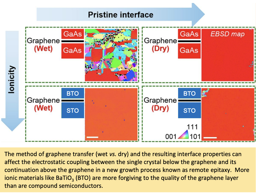
Remote epitaxy has drawn attention as it offers epitaxy of functional materials that can be released from the substrates with atomic precision, thus enabling production and heterointegration of flexible, transferrable, and stackable freestanding single-crystalline membranes. In this highlight, 2DCC and PARADIM team up to work with the inventor of remote epitaxy, Prof. Kim (MIT), to unveil the respective roles and impacts of the substrate material, graphene, substrate–graphene interface, and epitaxial material for electrostatic coupling of these materials, which governs cohesive ordering and can lead to single crystal epitaxy in the overlying film. We show that simply coating a graphene layer on wafers does not guarantee successful implementation of remote epitaxy, since atomically precise control of the graphene-coated interface is required and provides key considerations for maximizing the remote electrostatic interaction between the substrate and adatoms. The general rule of thumb discovered here enables expanding 3D material libraries that can be stacked in freestanding form. This work is published in ACS Nano 2021, 15, 6, 10587–10596.
CONTACT:
National Science Foundation
Division of Materials Research
2415 Eisenhower Avenue
Alexandria, VA 22314

Any opinions, findings and conclusions or recommendations expressed in this material are those of the author(s) and do not necessarily reflect the views of the National Science Foundation.
SOCIAL: